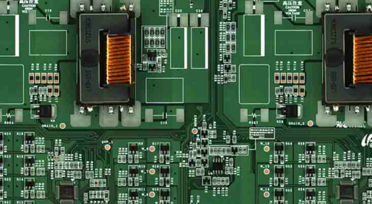
solder mask, it refers to the part of the board to get green oil. Because it is a negative output, the part of solder mask is not solder oil, but silver-white.
Welding aid
paste mask, which is used when the machine is pasting, is corresponding to the pad of all the components of the patch. The size is the same as the toplayer/bottomlayer layer, and it is used for opening the steel mesh and leaking tin.

Key points
The two layers are used for soldering on tin, not a tin, a green oil; So is there a layer refers to the layer of green oil, as long as there is a layer on an area, it means that the area is insulated green oil? I haven't come across such a layer yet! The solder plate on the PCB board we painted will all solder layer by default. Therefore, the solder plate on the PCB board manufactured is coated with silver solder, and it is not surprising that there is no green oil. However, the wiring part on the PCB board we drew only has toplayer or bottomlayer layer, rather than solder layer, but the wiring part of the PCB board made is coated with green oil. That can be understood this way:
1. The welding resistance layer means that the window is opened on the green oil of the whole piece of welding resistance, in order to allow welding!
2. By default, green oil should be applied to areas without solder resistance layer!
3. paste mask layer is used for patch encapsulation! SMT packaging uses toplayer layer, topsolder layer, and toppaste layer. toplayer and toppaste are the same size, but toppaste is larger than them. The DIP package is used only for: topsolder and multilayer layer (after decomposition, I found that multilayer is actually toplayer, bottomlayer, topsolder, bottomsolder layer overlapping), And topsolder/bottomlayer is larger than toplayer/bottomlayer.
Question: Is it correct to say "solder layer will only be plated if there is copper in it"? This is said by a man who works in the PCB factory. He means that if you want to solder the picture in the solder layer, you need to solder copper (in other words, there should be toplayer or bottomlayer in the area).
Now: I come to a conclusion: "solder layer will only be solder or gold plated if there is copper in it" is correct! solder layer refers to the area that is not covered in green oil!
mechanical, mechanical layer keepout layer top overlay top overlay screen layer bottom overlay top paste, bottom paste top solder layer bottom solder layer drill guide, bottom solder layer top solder layer drill guide, multilayer mechanical layer is to define the appearance of the entire PCB board, in fact, when we say the mechanical layer is referring to the overall structure of the PCB board.
The forbidden wiring layer is the boundary when we define the copper electrical characteristics in the laying, that is to say, after we define the forbidden wiring layer first, the wires with electrical characteristics that we lay cannot exceed the boundary of the forbidden wiring layer in the future laying process.topoverlay and bottomoverlay are the silk screen characters defining the top layer and the bottom layer. It's the component number and some characters that you usually see on a PCB board.
toppaste and bottompaste are the top layer of the bottom pad, which refers to the exposed copper and platinum that we can see. (For example, we drew a wire on the top wiring layer, and what we see on the PCB is just a wire, which is covered by the whole green oil. But we draw a square, or a point, on the toppaste layer where the line is, and the resulting board has no green oil on the square and on the point, but copper platinum.
The two layers top solder and bottomsolder are opposite to the previous two layers. You can say that these two layers are the layer to cover green oil. In fact, this layer is almost like the mechanical layer.
The top solder and bottomsolder layers are just the opposite of the previous two layers, so to speak, they are the layers to cover the green oil; Because it is a negative output, the part of solder mask is not solder oil, but silver-white.
1 Signal layer (Signal Layer)
The signal layer is mainly used to lay out the wires on the circuit board. Protel 99 SE provides 32 signal layers, including Top layer (top layer), Bottom layer (bottom layer) and 30 MidLayer (middle layer).
2 Internal plane layer (Internal Power supply/Connection layer)
Protel 99 SE provides 16 internal power layers/grounding layers. This type of layer is used only for multilayer panels, mainly for laying out power cables and ground wires. We call double layer, four layer, six layer, generally referring to the number of signal layer and internal power/connection layer.
3 Mechanical layer
Protel 99 SE provides 16 mechanical layers, which are commonly used to set board dimensions, data markers, alignment markers, assembly instructions, and other mechanical information. This information varies depending on the requirements of the design company or PCB manufacturer. Can perform menu commands Design | MechanicalLayer circuit boards set more mechanical layer. In addition, the mechanical layer can be attached to other layers together with the output display.
4 Solder mask layer (Solder mask layer)
Apply a coat of paint, such as anti-solder paint, to areas other than the pad to prevent tinning. The solder shield is used to match the pad during the design process and is automatically generated. Protel 99 SE provides Top Solder (top Solder) and Bottom Solder (bottom solder) layers.
5 Paste mask layer (Paste protective layer, SMD patch layer)
It is similar to the role of the solder resistance layer, the difference is that the corresponding surface paste type element in the machine welding pad. Protel99 SE offers two solder Paste protective layers, Top Paste (top layer) and Bottom Paste (bottom layer). Mainly for SMD components on PCB board. If the board is full of Dip (through-hole) components, the Gerber file output is not required for this layer. Before pasting SMD components on PCB board, each SMD pad must be coated with solder Paste. The steel mesh used for tinning must need the Paste Mask file, so that the film can be processed. The most important thing to be clear about Gerber output of Paste Mask layer is that this layer mainly aims at SMD element. Meanwhile, compare this layer with Solder Mask described above to get to know their different functions, because you can see the two film pictures are very similar.


