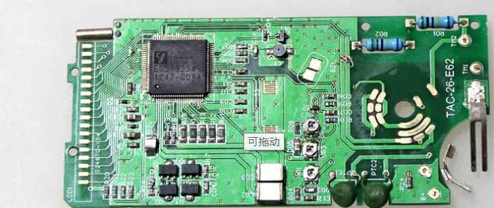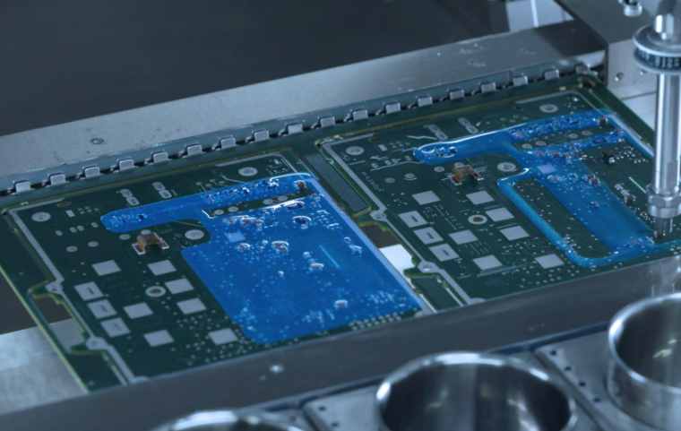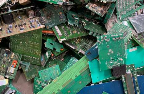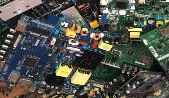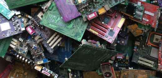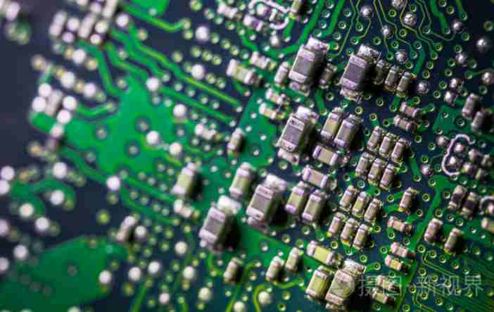
A Printed circuit board is found in almost every kind of electronic device. If there are electronic parts in a device, they are mounted on PCB boards of various sizes. In addition to fixing various small parts, the main function of PCB is to provide electrical connection between the above parts. With the increasing complexity of electronic equipment and the need for more and more parts,PCB board lines and parts are increasingly dense. A board with no parts on it is called a "bare board" and is often called a "printed circuit board" (PWB).
The PCB board itself is made of insulating, heat-resistant, and non-bendable material. The small circuit material seen on the surface of PCB board is copper foil. Originally, copper foil is covered on the whole board, but in the manufacturing process, the middle part is etched away, and the remaining part becomes a network of small lines. The lines are conductor patterns, or wiring, and are used to provide circuit connections for on-board parts of PCBS.
In order to secure the parts to the PCB board, we weld their pins directly to the PCB board. On the most basic PCB(single panel), the parts are concentrated on one side and the wires on the other. In this way, we need to make holes in the board so that the connector can go through the board to the other side, so the connector of the part is welded to the other side. Because of this, the front and back of PCB are called components (Component Side) and welding (Solder Side).
If there are some parts on the PCB board that need to be freely assembled and disassembled after production, the Socket will be used when the part is installed. As the socket is directly welded on the PCB board, the parts can be arbitrarily disassembled. For example, the ZIF(Zero Insertion Force) socket allows parts (in this case, the CPU) to be easily inserted into the socket or removed. A retaining rod next to the socket to hold the part in place after you plug it in.
If you want to connect two PCB boards to each other, we usually use the so-called "gold finger" side joint (edge connector). The finger contains a number of exposed copper pads that are actually part of the PCB wiring. Usually to connect, we insert the gold finger on one PCB into the appropriate Slot on the other PCB copy board (commonly called expansion Slot). In computers, interface cards such as video cards, sound cards, and the like are connected to the main board by the gold finger. The green or brown on the PCB board is the color of solder mask. This layer is an insulating protective layer that protects the copper wire and prevents parts from being welded in incorrect places. Another silkscreen will be printed on the solder resistance layer. It is usually printed with words and symbols (mostly white) to indicate the position of the parts on the board. Screen printing is also known as legend.
PCB board price factors
1. The different materials used for PCB board result in the diversity of price
Common double panel as an example, the board generally has FR4(Sheng Yi, King board, Guoji, three prices from the top down), the board thickness from 0.2mm to 3.0mm, copper thickness from 0.5oz to 3oz different, all these in a board caused a huge price difference; In terms of solder resistance ink, there is a certain price difference between ordinary the mo setting oil and photosensitive green oil.
2. Different surface treatment processes result in the diversity of prices
Common are :OSP(antioxidant), lead spray tin, lead-free spray tin (environmental protection), gold plating, gold sinking and some combination of processes, and so on, the more expensive the price of the above process.
3. Price diversity caused by different difficulty of PCB board itself
There are 1000 holes on both types of circuit boards. If the aperture of one board is larger than 0.2mm, the drilling cost will be different from that of the other board. For example, if two types of circuit boards are the same, but the line width and line distance are different, one is greater than 4mil, and the other is less than 4mil, the production cost will be different. Secondly, there are some ordinary plate process design is also charged money, such as half hole, buried blind hole, plate hole, press the keyplate printing carbon oil.
pcb_15.jpg
4. Different thickness of copper foil causes price diversity
Common copper platinum thicknesses are :18um(1/2OZ),35um(1OZ),70um(2OZ),105um(3OZ),140um(4OZ), etc. The higher the copper foil thickness, the more expensive.
5. Customer's quality acceptance standard
Commonly used are :IPC2, IPC3, enterprise standard, military standard and so on, the higher the standard, the higher the price will be.
6. Mold fee and test rack
(1) Mold cost. If the sample is in small batch, the plate factory generally adopts the drilling and milling shape, so that the milling cost will not be added. When doing a large batch, the mold is required to be opened and the plate is struck, so that there is a set of mold cost.
(2) test fee: the sample is generally used for flying needle test, and the test fee is generally charged by the board factory ranging from 100-400 yuan; Batch to open the test rack to test, test rack general plate factory quotation between 1000-1500 yuan.
7. Price differences caused by different payment methods
The less time it takes to pay, such as cash, the lower the price.
8. Order quantity/delivery time
(1) The less the quantity is, the more expensive the price will be, because even if it is to make 1PCS, the plate factory has to make engineering data and produce film, which process is necessary
(2) Delivery date: The data delivered to the PCB factory should be complete (GERBER data, the number of layers of the board, board, board thickness, surface treatment, ink color, character color and some special requirements should be written clearly).


