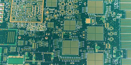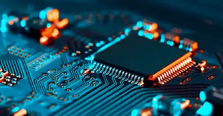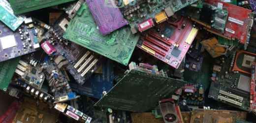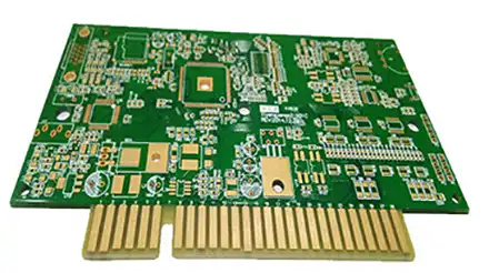
A multilayer PCB is a printed circuit board with more than 2 layers. Double-sided PCBs have two conductive layers on the top and bottom of the PCB substrate. Multilayer PCBs must have at least 3 layers of conductive material or copper. All layers are interconnected through copper plated vias. The number of layers can be 4, 6, 8...up to 40 layers.

Multilayer PCB designs are complex. The top and bottom layers look the same as a double-sided PCB, but with stacked layers on both sides of the core. All layers are compressed to form a single multilayer PCB where all layers are interconnected through copper plated vias.
All active and passive electronic components are assembled on the top and bottom layers. All internal stack layers are used for routing. Both through-hole electronic components and surface mount components (SMDs) can be soldered on either side of such PCBs. SMD components can be soldered using Surface Mount Technology and other PCBA tools. A typical multilayer printed circuit board has the following layer stackup:
Top layer (electronic components)
Inner 1 (routing)
Internal Layer 2 (Routing)
Inner Layer 3 (Routing)
Bottom layer (electronic components)
Multilayer PCB manufacturing process
The multi-layer PCB manufacturing process requires special attention as there are more opportunities for cross-connects, overlaps, traces, etc. in the copper areas. The entire process needs to be done in an ESD safe and clean room environment. The 8+ layer PCB manufacturing process requires special manufacturing setup and equipment.
Following are the steps involved in the multi-layer PCB manufacturing process:
The process starts with designing the PCB layout using any PCB design software/CAD tool (Proteus, Eagle, OrCAD).
The next step is to make the inner core. Laminates of the desired thickness are treated with copper foil, dry film resist, and UV light to make the inner core.
The next step is lamination. The process includes: inner core material, prepreg and copper foil. Sheets of material are stacked on top of each other and holes are used to align them as they stack.
For a 4-layer board, the layers are staked as follows: bottom layer of copper foil - prepreg - inner core - more prepreg - and finally copper foil on top.

The next step is to apply pressure, heat and vacuum using a heated hydraulic press. Vacuum is important to ensure that there is no air between the layers. This process will end within 2 hours, depending on the number of layers.
After curing, the resin from the prepreg joins the sheet, core and foil together to form a multilayer PCB.
Benefits of Multilayer PCBs
Reduced PCB size/small size (space saving).
light
High quality and high density
Better durability and flexibility
Powerful single connection point
Disadvantages of Multilayer PCBs
Higher manufacturing and production costs
complex design and production
limited manufacturer
Requires highly skilled and well-trained designers
Increase production time
Uses of Multilayer PCBs
Multilayer printed circuit boards offer greater flexibility and higher circuit density while being smaller in size. This is why many electronics companies around the world use these boards in several electronic devices and gadgets:
Computers and Laptops
Telecommunications Equipment - Cell Phones, Tablets and Other Hand Assist Devices
File servers and data storage
Signal transmission, mobile phone repeater, GPS
satellite
Medical equipment: tests, X-rays, heart monitors, CAT scans
Industrial equipment
nuclear system
Military and Defense Equipment
car
aerospace
Anywhere complex circuits are required.


