The PCB factory engineer explains Allegro's pad knowledge
circuit board manufacturing, circuit board design, PCBA processing manufacturers explain to you: circuit board factory engineers explain Allegro's pad knowledge
In Allegro, before making a part (Symbol), you must first establish the pin of the part. There are two types of component packaging: surface mount and in-line plug.
Different packages require different pads.
Padstack in Allegro mainly includes
1. Physical pads for components
1) Regular Pad. There are circles, squares, ellipses, rectangles, octagons, and arbitrary shapes (Shape)
2) Thermal Relief. There are circles, squares, ellipses, rectangles, octagons, and arbitrary shapes (Shape)
3) Anti Pad. Used to prevent pins from connecting to other networks. There are circles, squares, ellipses, rectangles, octagons, and shapes.
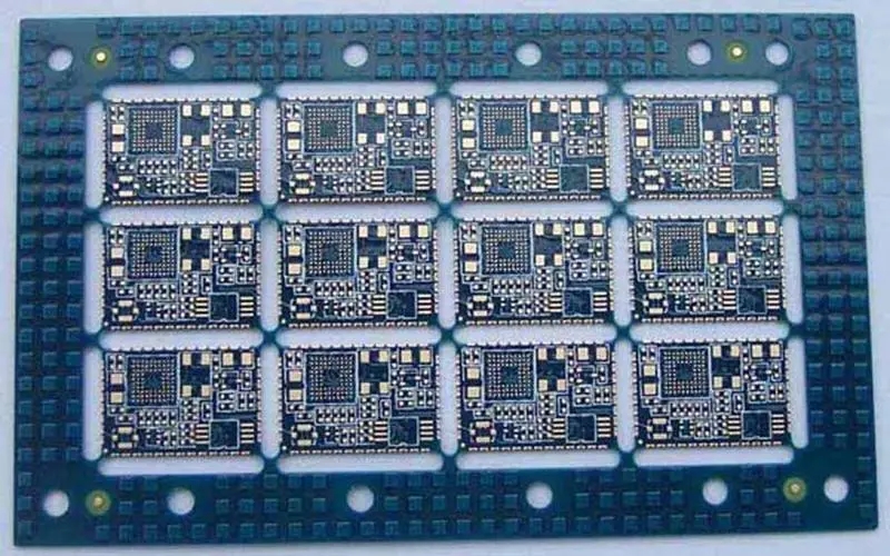
2. Soldermask:
Solder mask refers to the part of the board to be painted with green oil. In fact, the solder mask uses negative output, so after the shape of the solder mask is mapped to the board, it is not green oil solder mask, but copper skin is exposed. Generally, in order to increase the thickness of the copper sheet, the green oil is removed by scribing on the solder mask, and then tin is added to increase the thickness of the copper wire.
3. Pastemask:
It is used when the machine is mounted. In SMT processing, a steel plate is usually used to punch holes on the PCB corresponding to the bonding pad of components, and then solder paste is applied to the steel plate. When the PCB is under the steel plate, solder paste leaks, which means that each bonding pad can be coated with solder. Therefore, the solder mask cannot be larger than the actual size of the bonding pad. "<=" is the most appropriate.
4. Reserved layer (Filmmask)
Used to add user-defined information.
Packaging and bonding pad of surface mounted components, the layer and size to be set
Regular Pad:
The specific size is set according to the actual package size. It is recommended to refer to IPC-SM-782A Surface Mount Design and Land Pattern Standard.
Thermal Relief:
Generally, it is 20 mil larger than the regular pad size. If the Regular Pad size is less than 40 mils, the size difference needs to be appropriately reduced.
Anti Pad:
Generally, it is 20 mil larger than the regular pad size. If the Regular Pad size is less than 40 mils, the size difference needs to be appropriately reduced.
SolderMask:
Usually 4 mils larger than regular pads.
Pastemask:
Usually similar to regular pad size
Filmmask:
There are few applications. The user can set it himself.
The layers and dimensions to be set for the package pad of in-line components:
The required levels are almost the same as those of surface mount components, and the following main elements are required:
1. Begin Layer: Thermal Relief and Anti Pad are 0.5mm larger than the actual size of regular pads
2. End Layer: Thermal Relief and Anti Pad are 0.5mm larger than the actual size of regular pads
3. DEFAULT INTERNAL: M-server
Drilling size: actual PIN size+10mil
Pad size: at least drilling size+16mil (drilling size<50)
Pad size: at least drilling size+30mil (drilling size>=50)
Pad size: at least drilling size+40 mil (drilling is rectangular or oval)
Anti electric edge distance: drilling size+30mil
Solder resistance layer: regular pad+6mil
Flux: regular pad size
Inner hole size: drilling size+16mil
Outer hole size: drilling size+30mil
PCB manufacturers, PCB designers and PCBA manufacturers will explain to you: PCB factory engineers will explain Allegro's pad knowledge.


