Inspect PCB drawing and characteristics of soft and hard combination board
PCB manufacturers, PCB designers and PCBA manufacturers will explain and inspect PCB drawings and the characteristics of soft and hard combination boards
After the PCB wiring is completed, the design rules of the PCB should be checked to ensure that the PCB meets the design requirements and all networks are connected correctly. Then, how to check the correctness of PCB drawing design?
1. Whether the distances between wire and wire, wire and component pad, wire and via, component pad and via, and via and via are reasonable and meet Production requirements.
2. Whether to modify some undesirable lines.
3. Whether analog circuit and digital circuit have their own independent ground wires.
4. Whether the graphics (such as icons and labels) added in the PCB will cause signal short circuit.
5. Whether the outer frame edge of the power layer in the multi-layer circuit board is reduced.
6. Whether the width of the power line and ground wire is appropriate, whether the power line and ground wire are tightly coupled, and whether there are places where the ground wire can be widened.
7. Whether the best measures have been taken for the key signal lines, such as the shortest length, protection lines, etc.
8. Whether there is a process line on the PCB, whether the solder mask meets the requirements of the production process, whether the solder mask size is appropriate, and whether the character mark is pressed on the device pad.

The inspection results of design drawings can be divided into two types: one is report output, which generates a report of inspection results; The other is OnLine inspection, which is to inspect the electrical rules and wiring rules of the circuit board during the wiring process.
Characteristics of soft and hard combination plate
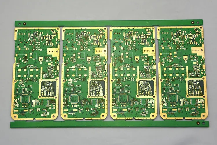
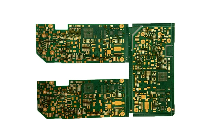
The birth and development of FPC and PCB gave birth to the new product of soft and hard combination board. Therefore, the soft and hard combination board is a PCB with FPC characteristics and PCB characteristics formed by combining the flexible PCB and the hard PCB according to relevant process requirements after pressing and other processes in PCB proofing.
In PCB proofing, the combination of soft and hard boards provides the best solution for limited space conditions. This technology provides the possibility of safely connecting equipment components while ensuring polarity and contact stability, and reduces the number of plugs and connector components.
Other advantages of the soft and hard combination board are dynamic and mechanical stability, resulting in 3D design degrees of freedom, simplified installation, space saving and maintenance of uniform electrical characteristics.
Soft and hard combination board The soft and hard combination board is expensive, but it has a wide range of uses, and can be customized for applications in many industries. There are several situations that make the soft and hard combination board the best solution. These include:
High impact and high vibration environment. The soft and hard bonding plate has a high impact resistance and can survive in a high stress environment, otherwise it will lead to equipment failure.
2. High precision applications where reliability is more important than cost considerations. If cable or connector failure is dangerous, it is better to use more durable hard and soft bonding plates.
3. High density applications: Some components lack the surface area required for all required connectors and cables. The soft and hard combination board can save space to solve this problem.
4. Applications requiring multiple rigid plates. When there are more than four connecting plates in the component, it may be the best choice to replace them with a single soft and hard combination plate, and it is more cost-effective.
PCB manufacturers, PCB designers and PCBA manufacturers will explain and inspect PCB drawings and the characteristics of soft and hard boards.


