The Development Trend of PCB in the Era of Internet of Things
According to PCB development, the era of Internet of Things has come, and it has occupied almost every aspect of the digital world
By using this technology, developers are developing smart connection platforms for wearable devices, home automation and medical monitoring systems, smart cars and future cities.
As the latest technology product, the Internet of Things has brought good performance for the connection between physical and digital components. This article will discuss the development and future of the Internet of Things in detail. Do you want to know more?
Internet of Things: A New Way to Promote PCB Development
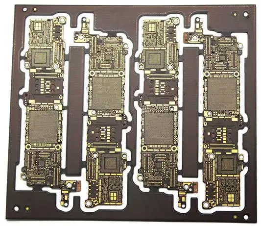
One of the main trends is PCB development today is the more and more wired use of flexible and high density interconnections (circuit board manufacturing. Traditional PCB wiring methods cannot achieve this. With HDI technology, such as blind holes and buried holes, in order to save expensive costs, HDI design can also help reduce power consumption and improve efficiency, making it an ideal choice for IoT devices
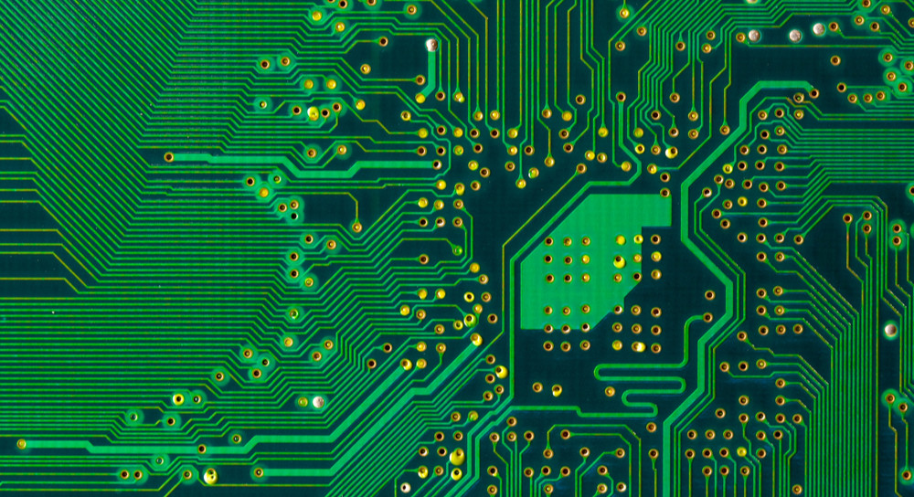
Circuit board

By integrating flex and HDI methods into PCB design, the company can manufacture micro mobile devices that are less affected by factors such as thermal stress and signal loss, without affecting their performance. IoT devices can now be smaller, lighter, and faster than ever before.
Making PCBs for the Internet of Things: What's the difference?
Although the Internet of Things does not require a complete transformation of PCB development, it brings new considerations to the design table.
Due to different design methods, the layout, manufacturing and assembly processes of printed circuit boards based on the Internet of Things are very different.
First of all, the Internet of Things PCB is usually composed of rigid and flexible or flexible circuit components, which is contrary to the large and flat characteristics of traditional circuit boards.
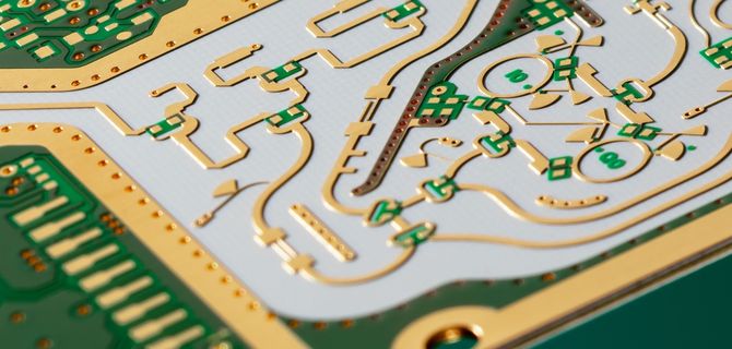
The use of flexible component manufacturing requires extensive and high-precision calculation of bending ratio, repeated calculation of life cycle, signal track thickness, rigid and flexible circuit layers, copper weight, stiffener placement and heat generated by components.
In addition, the development of IoT PCB requires designers to ensure the firm combination between rigid and flexible side layers, as well as in-depth understanding of very small components such as 0201 and 00105 packages.
In the future, FR4 designers will need to work with experts who know how to use alternative materials.
The research company is now the first choice for IoT developers to seek consulting and testing services for wireless autonomous sensors and flexible circuits.
Wireless modules and RF circuits provide IoT products with the key functions of communicating with the surrounding environment, collecting data and sending it to online and offline servers.
Today, the market is full of IoT friendly modules and RF components, all of which cover a small area and contain as many functions as possible.
However, with the development of world connectivity requirements, wireless technology will enter more and more small tools. PCB designers will have to face the challenge of installing more powerful and reliable modules on smaller circuit boards.
It may be necessary to modify and update the protocols for the specified range, data transmission speed, security and other parameters to meet the emerging requirements.
What is more exciting is that with standardization becoming the norm, a major wireless protocol is likely to dominate the future Internet of Things world.
More focus on power consumption
In the future, IoT products may eliminate physical power ports and plug-in power supplies and replace them with batteries and energy collection functions to promote portability and artificial intelligence.
The IoT market is increasingly eager for smart devices that can work continuously and hardly require human intervention. In order to succeed in the future, PCB designers need to pay more attention to energy efficiency.
A promising way to achieve better power consumption is to develop a power budget for each functional block on the PCB, rather than considering the product as a whole. In this way, designers will gain much-needed flexibility to identify and improve consumers.
Human PCB
As IoT developers find new ways to improve their daily lives, the number of health and fitness electronic products is increasing every year. However, the human body poses some unique challenges to PCB designers.
For example, the extreme fatigue of our bodies means that any device that we intend to wear or put in our pocket needs to maintain a strong enough signal to overcome noise.
In addition, since moisture and circuit will not mix, the design of wearable devices for the Internet of Things requires developers to carefully consider the impact of sweat.
Mechanical engineers play an important role in the development of moisture-proof packaging, but with the increasing use of Internet of Things gadgets, PCB designers will need to do more to ensure that sensitive components are well protected.
Stronger reliability
Small IoT devices require very high manufacturing accuracy. Although most designers are usually used to replacing fried through-hole components on traditional circuit boards, the IoT market cannot tolerate failure.
Sensitive devices such as watches and hearing aids must always work.
As the demand for IoT products continues to rise, PCB designers need to ensure that their circuit boards are ready for use out of the box.
This means that before starting physical manufacturing, a lot of time is spent on analog programs, such as PSpice, to carefully optimize its prototype to obtain the best performance.
In short
In order to keep up with the pace of the Internet of Things, electronic design is undergoing tremendous changes The new method is occupying the central position, and PCB manufacturers are gradually considering overall product development, not just circuit board design
As the demand for powerful circuit boards with miniature and lightweight components expands, designers and manufacturers with the imagination and expertise to take advantage of emerging opportunities will benefit greatly.


