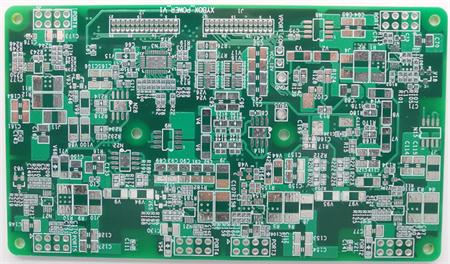
In the actual PCB circuit design, we will use one or more of the following methods for static protection:

1. Avalanche diode for static protection
This is also a method often used in the design. The typical method is to connect an avalanche diode in parallel on the key signal line to the ground. This method utilizes avalanche diode's fast response and stable clamping ability, which can consume accumulated high voltage in a short time to protect the PCB.
2. Circuit protection using high-voltage capacitors
In this practice, the ceramic capacitor with a withstand voltage of at least 1.5KV is usually placed at the I/O connector or key signal position, and the connecting line is as short as possible to reduce the inductance of the connecting line. If a capacitor with low withstand voltage is used, the capacitor will be damaged and the protection will be lost.
3. Use iron oxide magnetic beads for circuit protection
Iron oxide magnetic beads can attenuate ESD current and inhibit radiation. When faced with two problems, a ferrite bead is a good choice.
4. Spark gap method
This method is seen in a piece of material. The specific method is that the microstrip line layer composed of copper sheets is composed of triangular copper sheets whose tips are aligned with each other. One end of the triangular copper sheet is connected to the signal line, and the other is connected to the ground. When there is static electricity, it will produce tip discharge and then consume electric energy.
5. Adopt the method of LC filter to protect the circuit
LC filter can effectively reduce high-frequency static electricity entering the circuit. The inductive reactance of the inductor can well prevent high-frequency ESD from entering the circuit, while the capacitor shunts the high-frequency energy of ESD to the ground. At the same time, this type of filter can smooth the signal edge with less RF effect, and its performance has been further improved in signal integrity.
6. ESD protection with multilayer boards
With the permission of funds, selecting multilayer boards is also an effective means to prevent ESD. In the multilayer board, since there is a complete ground plane close to the wiring, ESD can be more quickly coupled to the low impedance plane, thus protecting the role of key signals.
7. The method of leaving protective tape around the PCB
This method is usually used to draw wiring without assembly and welding layer around the PCB. If conditions permit, connect the wiring to the housing. At the same time, note that the wiring cannot form a closed loop, so as to avoid causing more trouble by forming a loop antenna.
8. CMOS devices with clamping diodes or TTL devices are used for circuit protection
This method uses the isolation principle to protect the PCB. Because these devices are protected by clamping diodes, the complexity of the design is reduced in the actual circuit design.
9. Decoupling capacitor is often used
These decoupling capacitors should have low ESL and ESR values. For low-frequency ESD, the decoupling capacitors reduce the area of the loop. Because the role of its ESL weakens the role of the electrolyte, it can better filter out high-frequency energy.
In a word, although ESD is terrible, it may even bring serious consequences. However, only by protecting the power supply and signal lines on the circuit, the ESD current can be effectively prevented from flowing into the PCB. Among them, my boss often said that "a good grounding of a board is the king's way", and I hope that this sentence can also bring about the effect of breaking the skylight.


