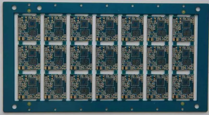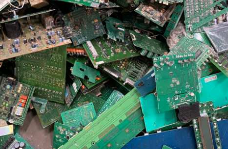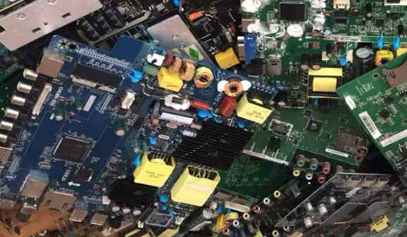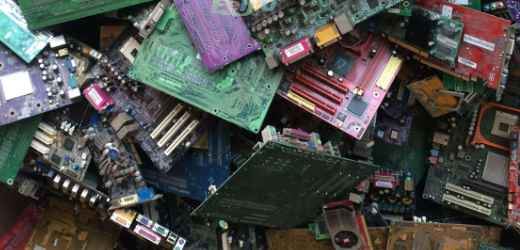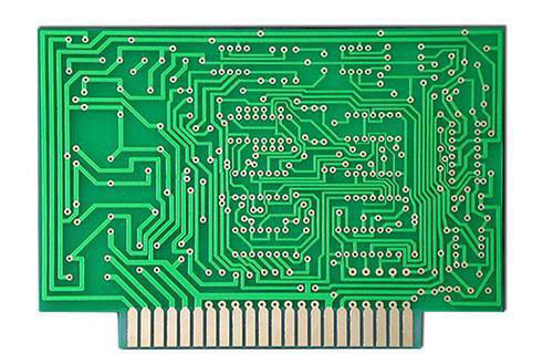
Moisture is the most common and destructive factor to PCB. Excessive moisture will greatly reduce the insulation resistance between conductors, accelerate high-speed decomposition, reduce Q value, and corrode conductors. We often see that the patina on the metal part of PCB is caused by the chemical reaction of the metal copper with water vapor and oxygen, which is not coated with three proofing paint. And hundreds of pollutants found on printed PCBs have the same destructive power. They will lead to the same result as that caused by moisture erosion - electronic deterioration, corrosion of conductors and even irreversible short circuits.

So what does the "three proofing" paint for circuit board mean? What is the relevant process? Now Shenya will take you to understand the function and process of the three proofing paint.
What does the "three proofing" paint for circuit board refer to?
There are mainly three kinds of three proofing treatment processes for PCB: three proofing paint, electronic wax and nano coating.
The three proofing paint for PCBs, also known as the three proofing paint for PCBs, is a specially formulated paint used to protect PCBs and their related equipment from the corrosion of bad environments, thus improving and extending their service life and ensuring the safety and reliability of use. The three proofing paint for circuit board can be divided into acrylate, silicone and polyurethane from the chemical composition. Brush coating, spraying, soaking and other processes are generally adopted. After the coating is dried and solidified, a protective film will be formed to protect the circuit board from moisture, salt spray and mold. This is also the most widely used three prevention process in the electronic industry.
Application process of three proofing paint
1. Brush coating - it is widely used and can produce excellent coating effect on smooth surface.
2. Spraying - the use of spray can type products can be easily applied to maintenance and small-scale production. The spray gun is suitable for large-scale production, but these two spraying methods have high requirements for the accuracy of operation, and may produce shadows (where the lower part of the components is not covered with three proofing paint).
3. Automatic dip coating - dip coating can ensure complete film covering without causing material waste due to overspray.
4. Selective coating - coating is accurate and does not waste materials. It is suitable for coating in large quantities, but has high requirements for coating equipment. It is most suitable for film covering in large quantities.
technological requirements
1. First of all, the circuit board shall be cleaned and dried to remove moisture and moisture. The dust, moisture, oil stain, flux and solder paste on the surface of the object to be coated must be removed first, so as to give full play to its protective effect. Thorough cleaning can ensure that the corrosive residues are completely removed and the three proofing paint is well adhered to the surface of the circuit board. Baking conditions: 60 ° C, 10-20 minutes, after taking out in the oven, the coating effect is better when hot.
2. The brushing method shall be used for coating, and the brushing area shall be larger than the area of the device to ensure that all devices and pads are covered.
3. The plate shall be laid flat as far as possible during brushing, and there shall be no dew after brushing. The brushing shall be smooth, and there shall be no exposed part, which is better between 0.1-0.3mm.
4. Before brushing and spraying, the diluted product shall be fully stirred, and it shall be sealed for 2 hours before brushing or spraying to avoid solvent volatilization. Use a high-quality natural fiber brush to gently brush and dip at room temperature. If a machine is used, the viscosity of the coating shall be measured (with a viscosity agent or flow cup), and the viscosity can be adjusted with a thinner.
5. After brushing, lay it flat on the support to prepare for curing. Heating is required to accelerate the curing of the coating. If the coating surface is uneven or contains bubbles, it shall be cured in a high temperature furnace for more time at room temperature to allow the solvent to flash out.
6. During dip coating, the circuit board components shall be vertically immersed in the three proofing paint bath, and the connectors and related components shall not be immersed. Unless carefully covered, the circuit board shall be immersed for 1 minute until the bubbles disappear, and then slowly taken out. A uniform film will be formed on the surface of the circuit board. Most of the three proofing paint residues shall flow back from the circuit board to the dip coater or dip coater. The immersion of electronic PCBs or components should not be too fast to avoid excessive bubbles.
7. If there is skin on the surface after dip coating, remove the skin and continue to use.
Parts and devices that cannot be coated with three proofing paint
1. Conventional non coating devices: painted high-power radiator, radiator, power resistor, high-power diode, cement resistor, pullout switch, potentiometer (adjustable resistor), buzzer, battery base, fuse base, IC base, touch switch, relay and other types of sockets, pins, terminal blocks, DB9, plug-in or patch type LED (non indicating), digital tubes, and grounding screw holes.
2. The parts and components specified in the drawing that cannot be painted with three proofing paint.
3. It is stipulated in the list of "Non three proof Components (Areas)" that the three proof paint cannot be used for the components. If the conventional non coating devices specified in the regulations need to be coated, the R&D department can specify the requirements or drawings to mark the "three proofing" coating.
The above is an introduction to what is the three proofing paint for PCBs, its function and process


