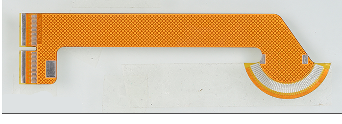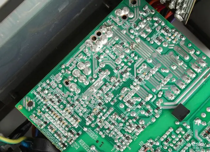
The soft and hard combination board has the characteristics of FPCand PCB at the same time. Therefore, it can be used in some products with special requirements, including a certain flexible area and a certain rigid area. It is very helpful to save the internal space of the product, reduce the volume of the finished product, and improve the performance of the product. The mobile version is commonly used.
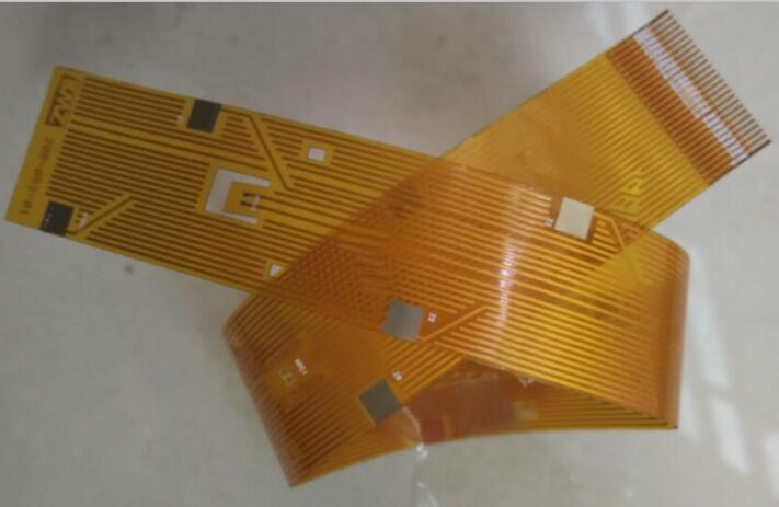
There are many production processes for soft and hard bonding plates, which are difficult to produce, low yield, and more materials and manpower. Therefore, the price is relatively expensive and the production cycle is relatively long.
For our PCB design engineers, in the process of welding, the soft and hard plates are assembled together. We place and weld the components on the hard board. For some products, components need to be welded on the flexible plate. In this case, a hard plate should be reserved under the flexible plate to support the flexible plate. The hard plate is not pasted with the flexible plate, and its contour is milled with a milling cutter with controllable depth. When the welding is completed, workers can press it down with their hands. We just need to distinguish our soft and hard parts and tell the processing plant.
In PCB design, we need to pay attention to: do not bend at the corner, use arc routing, do not use 45 degree routing and our right angle acute angle routing here, and do not suggest sudden changes in the routing width. There will be a weak force point for the soft board, and problems will occur in the later stage if we are not careful. The soft board is paved with copper, and the copper filling here is treated with grid copper skin. The pad on the flexible board must be larger than the pad on the typical rigid board. The device density of the circuit cannot be too high. These are caused by its own factors. The designer should pay attention to them when designing. At the same time, for flexible boards with double-sided layout, the layout should also be staggered and symmetrical.
In terms of layout, when the size of Flexible circuit board is too large, although the welding is easier to control, the printing line is long, the impedance increases, the anti noise ability decreases, and the cost increases; If it is too small, the heat dissipation will drop, the welding is not easy to control, and adjacent lines are prone to interfere with each other, such as electromagnetic interference of flexible circuit board. Therefore, the flexible circuit board design must be optimized:
(1) Shorten the connection between high-frequency components and reduce EMI interference.
(2) Components with large weight (such as more than 20g) shall be fixed with supports and then welded.
(3) Heat dissipation shall be considered for heating elements to prevent large Δ In case of defects and rework, the thermal sensor shall be far away from the heat source.
(4) The arrangement of elements shall be as parallel as possible, which is not only beautiful but also easy to weld, and it is suitable for mass production. The PCB circuit board is designed as a 4:3 rectangle (preferred). The wire width shall not be abrupt to avoid the discontinuity of wiring. When the circuit board is heated for a long time, the copper foil is easy to expand and fall off. Therefore, large area copper foil should be avoided.


