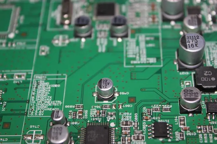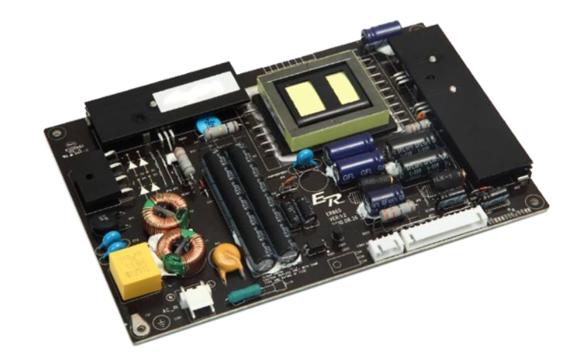
PCB design has developed from single-layer to double-layer, multi-layer and flexible, and still maintain their own trends. Due to the continuous development of high precision, high density and high reliability, the size is reduced, the cost is reduced, and the performance is improved, so that the printed circuit board will remain strong vitality in the future development of electronic equipment.
Simply teach you how to complete PCB design!
1. Prepare in advance
Prepare component libraries and schematics. Before continuing PCB design, first prepare SCH schematic component library and PCB component package library.
The PCB design component package library is preferably constructed by engineers based on the standard size data of the selected components. In principle, the component package library of PC shall be established first, and then the schematic SCH component library shall be established.

PCB design component packaging library has high requirements, which will directly affect the installation of PCB; The schematic SCH component library is relatively loose, but pay attention to defining pin attributes and the corresponding relationship with PCB component package library.
2. PCB structure design
According to the determined board size and various mechanical positioning, draw the PCB frame in the PCB design environment, and place the required connectors, key switches, screw holes, assembly holes, etc. according to the positioning requirements.
Fully consider and determine the wiring area and non wiring area (for example, the scope of screw hole is non wiring area).
3. PCB design layout
Layout design is to place components in PCB frame according to design requirements. Generate the network table in the schematic tool (Design → CreateNetlist), and then import the network table in the PCB software (Design → ImportNetlist). After the network table is successfully imported, it will exist in the software background. Through Placement operation, all devices can be called out, and a flying wire prompts connection between each pin. At this point, the equipment can be arranged.
PCB layout design is the first important process in the whole PCB design process. The more complex the PCB board is, the layout will directly affect the implementation simplicity of post wiring.
Layout design depends on the circuit foundation and design experience of circuit board designers, which is a high-level requirement for circuit board designers. The main circuit board designer has a light experience, which is suitable for small module layout design or PCB layout design tasks, and has low circuit board difficulty.
4. PCB layout design
PCB layout design is the most labor-intensive process in the whole PCB design, which directly affects the performance of PCB.
In PCB design, there are usually three areas of wiring:
The first is Butong, which is the most basic introduction requirement for PCB design;
Secondly, the electrical performance is satisfied. This is the standard for measuring whether PCB boards are qualified. After wiring, carefully adjust the wiring to obtain the best electrical performance.
Finally, it is clean and beautiful, and the wiring is messy. Even if the electrical performance is passed, it will bring great inconvenience to the later transformation optimization and test maintenance. The wiring shall be neat and uniform, and the vertical and horizontal wiring shall be irregular.


