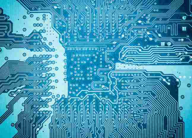
PCB is short for printed circuit board (Printed CircuieBoard). Usually on the insulation material, according to the predetermined design, made of printed circuit, printed components or a combination of the conductive graphics known as printed circuit. The conductive pattern that provides the electrical connection between components on the insulating substrate is called the printed line. In this way, the printed circuit or printed circuit of the finished board called printed circuit board, also known as printed board or printed circuit board.
PCB almost all the electronic equipment we can see can not be separated from it, as small as electronic watches, calculators, general computers, as large as computers, communication electronic equipment, military weapon systems, as long as there are integrated circuits and other electronic devices, electrical interconnection between them to use PCB. It provides mechanical support for the fixed assembly of various electronic components such as integrated circuits, realizes wiring and electrical connection or electrical insulation between various electronic components such as integrated circuits, and provides the required electrical characteristics, such as characteristic impedance. At the same time to provide solder resistance pattern for automatic solder welding; Provide identification characters and graphics for component assembly, inspection and maintenance.

How are PCBS made? We open the keyboard of a general-purpose computer and see a soft film (flexible insulating material) printed with a silver-white (silver paste) conductive pattern and a health pattern. Because of the general screen leakage method to get this pattern, so we call this printed circuit board flexible silver printed circuit board. And we go to the computer city to see a variety of computer host boards, graphics cards, network cards, modems, sound cards and household appliances on the printed circuit board is different. The substrate used is made of paper base (usually used for single side) or glass cloth base (usually used for double side and multilayer), prepreg phenolic or epoxy resin, one or both surface layers glued to a copper sheet and then laminate and cure. This kind of circuit board covered with copper sheet plate, we call it rigid plate. To make printed circuit board, we call it rigid printed circuit board. Single-side printed circuit board we call single-side printed circuit board, double-side printed circuit board, and then through the metallization of the hole for double-side interconnection, we call it a double panel. If a double-sided for the inner layer, two single-sided for the outer layer or two double-sided for the inner layer, two single-sided for the outer layer of the printed circuit board, through the positioning system and insulating binder material alternating together and conductive graphics in accordance with the design requirements of the interconnected printed circuit board will become a four-layer, six-layer printed circuit board, also known as the multi-layer printed circuit board.
There are now over 100 layers of functional printed circuit boards.
PCB production process is more complex, it involves a wide range of processes, from simple mechanical processing to complex mechanical processing, there are ordinary chemical reactions and photochemical electrochemical thermal chemistry and other processes, computer aided design CAM and other aspects of knowledge. In addition, there are many technological problems in the production process and new problems will be encountered from time to time. Some of the problems will disappear without finding out the causes. Because the production process is a discontinuous assembly line, any problem at any link will result in the whole line being stopped or a large number of scrapped consequences. Process engineers can be stressful, so many engineers leave the industry to work in sales and technical services for PCB equipment or materials companies.
Surface mounting technology has the following advantages:
1) Because the PCB eliminates large pass-through hole or buried hole interconnection technology, the wiring density on the PCB is improved, the PCB area is reduced (generally one of the third steps of plug-in installation), and the number of design layers and cost of the PCB are also reduced.
2) Reduce the weight, improve the seismic performance, the use of colloidal solder and new welding technology, improve product quality and reliability.
3) Due to the increase of wiring density and the shortening of lead length, the parasitic capacitance and inductance are reduced, which is more conducive to improving the electrical parameters of the printed board.
4) It is easier to realize automation than plug-in installation, improve installation speed and labor productivity, and correspondingly reduce assembly cost.
From the above surface safety technology can be seen, the improvement of circuit board technology is the improvement of chip packaging technology and surface installation technology. Now we look at the computer board card surface adhesion rate is constantly rising. In fact, this kind of circuit board with transmission screen printing line graphics is unable to meet the technical requirements. Therefore, the common high precision circuit board, its circuit graphics and solder graphics basically use sensitive circuit and sensitive green oil production process.
With the development trend of High Density Circuit Boards, the Production requirements of circuit boards are becoming higher and higher. More and more new technologies are applied to the production of circuit boards, such as laser technology, photosensitive resin and so on. The above is just a few superficial introduction, there are many things in the production of circuit board due to space constraints did not explain, such as blind hole, wound board, Teflon board, lithography technology and so on. If you want to go deeper, you need to make your own efforts.


