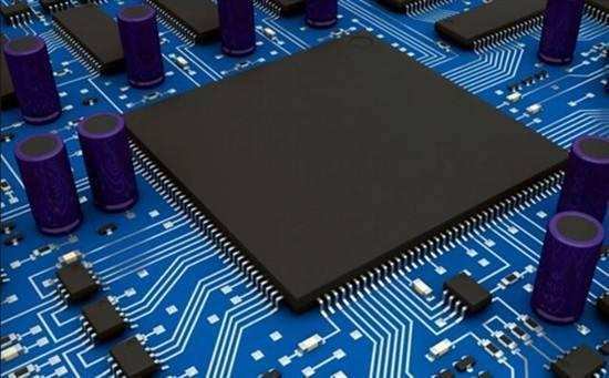
Basic principles of layout
1. Communicate with relevant personnel to meet special requirements of structure, SI, DFM, DFT and EMC.
2. According to the structural element diagram, place the devices that need to be located, such as connectors, mounting holes and indicators, and give these devices immovable attributes and dimensional labeling.
3. According to the special requirements of the structural elements diagram and some devices, set up no wiring area and no layout area.
4. Considering PCB board performance and processing efficiency, select the process flow (single-side SMT is preferred; Single-side SMT+ plug-in; Double-sided SMT; Double-sided SMT+ plug-in), and according to different processing characteristics layout.
5, layout reference to the results of the pre-layout, according to the "first big after small, first difficult after easy" layout principle.
6. The layout should meet the following requirements as far as possible: the overall connection is as short as possible, and the key signal line is the shortest; High voltage and high current signals are completely separated from weak signals of low voltage and low current signals; Analog signals are separated from digital signals; High frequency signals are separated from low frequency signals; The spacing between high-frequency components should be sufficient. On the premise of meeting the requirements of simulation and timing analysis, local adjustment.
7, the same circuit as far as possible using symmetrical modular layout.
8. The recommended grid for layout is 50mil, and the recommended grid for IC device layout is 25 25 25 mil. When the layout density is higher, the grid setting of small surface mount devices is recommended to be no less than 5mil.
9. In the layout, consider the position of fanout and test point, move with reference to the central point of the device, and consider running two wires in the middle of the two holes.
General rules for PCB wiring
1. The number of layers of printed wire wiring shall be determined according to needs. Wiring occupied channel ratio should generally be more than 50%;
2, according to the process conditions and wiring density, reasonable selection of wire width and wire spacing, and strive for uniform wiring within the layer, the wiring density of each layer is similar, when necessary, the lack of line area should be added auxiliary non-functional connection disk or printed wire;
3, the adjacent two layers of wire should be distributed into each other vertical oblique or curved line, to reduce the parasitic capacitance;
4, printed wire wiring should be as short as possible, especially high frequency signal and highly sensitive signal lines; For important signal lines such as clocks, equal delay wiring should be considered when necessary;
5. When a variety of power sources (layers) or ground (layers) are deployed on the same layer, the separation spacing should not be less than 1mm;
6. For large area conductive graphics larger than 5×5mm², the window should be partially opened;
7. Thermal isolation design should be carried out between the large area graphics of the power layer and the formation and its connecting disk.

Cable width/distance
1. The recommended line width/spacing for PCB processing is not less than 5mil/5mil, and the minimum usable line width/spacing is 4mil/4mil.
2. Distance between wiring and pad: the distance between outer wiring and pad is consistent with the distance between inner wiring and hole ring.
3. The distance between the outer wiring and the welding pad must meet the requirement that the distance between the wiring and the welding pad welding window edge is not less than 2mil.
Safe distance from the line
1. The distance between the cable and the edge of the plate is > 20mil. Inner power supply/ground distance from board edge > 20mil.
2. The distance between grounding busbar and grounding copper foil should be > 20mil.
3, in the metal shell (such as: radiator, power module, metal handle bar, horizontal voltage regulator, crystal vibration, ferrite inductance, etc.) directly contact with the printed circuit board area is not allowed to run. The area extending 1.5mm outward from the contact area between the metal shell of the device and the PCB is the surface cabling forbidden area.
The closest distance between the cable and the nonmetallic hole
General principles of multilayer PCB layering
1. The ground plane (the second layer) below the device surface provides the device shielding layer and the reference plane for the wiring of the device surface;
2. All signal layers are adjacent to the ground plane as far as possible;
3, try to avoid the two signal layers directly adjacent;
4. The main power supply should be adjacent to it as far as possible;
5. In principle, symmetrical structure design should be adopted. The meaning of symmetry includes: medium layer thickness and type, copper foil thickness, graphics
Symmetry of distribution types (large copper foil layer, line layer).
General requirements for silk screen design
1. In order to ensure that all letters, numbers and symbols can be easily identified on the PCB, the line width of the silk screen must be greater than 5mil and the height of the silk screen must be at least 50mil.
2. Screen printing is not allowed to overlap with pad and reference point.
3, white is the default color of silk screen printing ink, if there is a special need, need to be explained in the PCB drilling drawing file.
4. In the design of high density PCB circuit board, the content of screen printing can be selected according to the need.
5, silk screen string arrangement direction from left to right, from bottom up.


