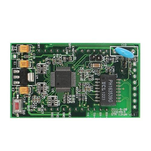
When laying out PCB board, you should pay attention to some key points of PCB board. Although we might think of it when designing individual printed circuit boards, the reality is that boards are often arranged in panels to help reduce production costs. Let's take a look at what a PCB panel is and then look at the eight PCB board guidelines you should know about board design.

The basis of PCB board
A PCB board is a large piece of circuit board material that can accommodate multiple individual circuit board instances. By paneling multiple PCBS at once, manufacturers and assemblers can reduce overall manufacturing costs for customers. Another benefit is that the panel size is more appropriate for manufacturing operations and will help reduce manufacturing and assembly defects.
The panel process begins with a manufacturing process in which images of individual panels are copied to fit standard panel sizes. Once the panels are manufactured, they will be sent to an assembler where the parts will be installed and welded. When the fabrication of the panels is complete, the boards are de-paneled, which means they are broken down into individual printed circuit board components. Panels are a normal part of the circuit board manufacturing process, but designers should pay attention to some details that will help panel their PCB designs.
Eight PCB panel guide
Panel sizes: Manufacturers use different panel sizes, some of which are more common than others. The size of the board will have a big impact on which panel size is ultimately chosen, depending on how it is laid out in the panel.
Layer stacking: One of the advantages of a panel is that multiple boards can be arranged in it, but layer stacking must be uniform for all boards.
Structure: Instances of the board need to have specific gaps between each other and the edge of the panel, and will typically include alignment holes and other features.
Layout: The circuit board is usually placed to maximize the available space in the panel, but it all depends on the orientation of the board during soldering. In some cases, circuit boards must be arranged to achieve optimum weldability.

Breakout: In order to get the finished board off the panel, a V-shaped slot or "Breakout" TAB will be used to configure the edge of the board. The designer needs to know what will be used to place the components correctly. When using V-grooves, there should be at least 0.075 inches between the edges of the board and the assembly, and 0.125 inches between the splitter. These gaps are necessary to prevent the solder joints from cracking during the de-paning process.
Component gaps: Breakouts are not the only component gaps that designers need to be aware of. Components that hang above the edge of the plate also require additional clearance, depending on the manufacturing process. Larger components will also require more clearance at the edges of the board than the minimum clearance already specified for V-slots and paging lugs.
Tools: The panel will need its own tool holes and benchmark markers, which should match the content on the board.
Physical support: Due to their thickness and overall size, certain PCB boards may require additional support to prevent sagging during manufacturing. This is done by adding brackets to the panel, which may be affected depending on the layout of the panel.
Following these guidelines with your PCB partner manufacturer can help you avoid problems when you panel your board.Should PCB designers lay out their own panels? Although PCB designerscan make their own panels, contract manufacturers are generally recommended to carry out this work.


