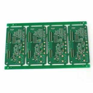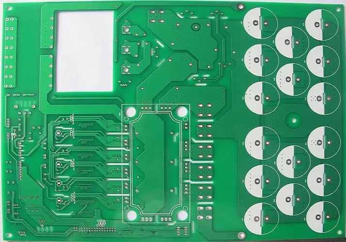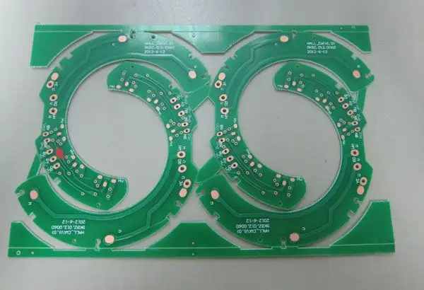
PCB production uses correct design tools to avoid PCB layout errors
The layout of printed circuit board is a difficult and arduous task, please do not let others tell you. The circuit must be structurally designed according to strict rules to operate at the highest performance, and at the same time, another set of design rules must be followed to achieve manufacturability. Even small and "simple" layouts can pose unique design challenges, and PCB layout engineers must be equipped with the latest tools to complete their work.
The CAD tool for PCB design is a miracle of software engineering. They have many different features and functions, so that layout designers can complete their work. These range from utilities to the design of the initial setup layout to the advanced trace routing engine to complete all network connections of the schematic. In order to make the best use of these tools, designers must understand all the nuances of PCB layout, especially those that can cause problems if not handled properly. These are some common PCB layout errors that designers should pay attention to.
Ready to design: Are you ready for PCB layout?
When the new design is ready for layout, it's natural to jump in and start placing components and routing tracks. The problem with this is that you usually need to do a lot of preparation before the layout starts. Many designers fall into the trap of "I'll deal with it later", but find that they now have bigger problems to correct, which could have been avoided if they had prepared better. The following are some common problems. If you solve them in advance, you can avoid many troubles in the future.
Out of date or incorrect components: It is not uncommon for a schematic component to have problems. If they copy the circuit from an earlier design, or the library is not up to date, or use a collection of actually outdated components, the final result will be the same. These components may not be available for manufacturing, so they need to be redesigned to update the parts. Cleaning up such errors in the BOM or using parts in the library service can solve this problem.
Incorrect design synchronization: Sometimes design work starts even if the schematic database is not fully synchronized with the layout. There are many convincing reasons for this, among which time saving ranks first, but the effect is often poor. The synchronization problem must be corrected later, which may cause some parts of the complete circuit to be torn. The lesson here is to spend some time making it right, and then spend too much time on layout.
Circuit board layer stacking configuration: As we all know, designers will begin to layout the circuit board before the layer stacking is finally determined. Again, this is usually to save time, but these good intentions can backfire. After the layout starts, moving layers around in the CAD system may take some time and may lead to design errors. However, the bigger problem is whether moving the completed wiring from one layer to another will affect the overall signal integrity of the circuit board. You may find yourself having to redesign some major parts of the circuit to correct these problems.
Design parameters: Failure to fully set PCB design CAD system before the start of layout may not introduce design errors, but may slow down your speed. Colors, meshes, and many other parameters are designed to create a work environment that helps improve productivity, and if you do not configure these parameters before you begin, you will only harm yourself. Many of these settings can be transferred in templates or readme files, which is very helpful when starting a new design.

At this point, the board is ready to begin layout. Next, we will examine some common errors that can occur during component placement.
PCB layout error when placing components
Let's face it. Although it may be very complicated, PCB layout is also very interesting. Manipulating components on the screen and binding them with a mesh connecting rubber band is one of the best and most challenging problems you can solve. However, just like setting before placing boards, if you do not take precautions, there are some potential problems that may cause many problems in your design. Let's start with a potential problem involving the physical footprint you will place on the board.
Incorrect footprints: We have discussed the importance of using correct components in design, but if these components use incorrect footprints, you will still encounter problems. Although technically this should be discovered during design synchronization, designers should ensure that they are using the correct encapsulation. Whether PQFP is used to replace BGA or capacitor polarity is reversed, if such error is not found immediately, it needs to be redesigned.
Don't ignore the plan: In order to ensure good signal and power integrity, PCB design circuits must be carefully divided to achieve the best performance. This is especially true for high-density designs that are important per millimeter of space. Designers who fail to do this may need expensive redesign to improve the performance of the circuit board. Using a schematic to place components of a logical group or specifying placement rooms on a board can be very helpful in preventing zoning errors.
DFM is essential: ensuring the manufacturability of the circuit board is as important as the signal and power integrity in the design. It is essential that PCB designers follow the rules of manufacturability in layout (DFM) for design. This includes the minimum spacing between components for automatic assembly equipment and test equipment, as well as space for technicians to debug and rework circuit boards. The use of design rules and constraints in CAD tools is absolutely necessary to eliminate DFM errors.
Remember to design the PDN: Although the layout of the circuit board is critical to ensure good signal integrity, it is equally important to focus on the Power Transmission Network (PDN). When laying out power components, designers can easily relax their efforts to introduce noise and other disturbances into the design. Ensure that good PDN design guidelines are followed and errors are checked using the power integrity tools of the CAD system.
Finally, the circuit board can be wired, but please do not relax your vigilance. If you are not careful, errors may still spread to the design.
Routing on PCB layout is a very meaningful task. After each routing is completed, its corresponding network connection guide will be eliminated, so that you can further complete the work. Design errors are also easy to spread, because they can damage the work you are trying to accomplish, so designers must be vigilant. Here are some examples to note.
Escape wiring: surface mount devices need to route wires from their pads to through holes to interconnect on other layers of the board. This is called escape routing or fan out routing, which is very simple for most SMT devices. However, high pin count devices with small spacing pose a greater challenge. Designers must be careful not to block the wiring channels on the internal layer through escape vias. Typically, chip manufacturers publish recommended cabling solutions in their product data sheets, which can help you avoid cabling congestion.
Constraint Management: Given all the different requirements of today's board design, layout designers must make full use of their design constraint management system. These utilities allow you to configure the necessary routing width and spacing for a network or group of networks, and to assign clearance rules to components. They can even go further by setting high-speed design topology, through-hole type and electrical timing parameters. In the figure above, you can see some settings available in the design constraint management system to prevent violation of routing rules.
There is not enough cabling space: it is very important to plan the location of cabling in advance when wiring the circuit boards with dense wiring patterns. This will ensure that there is enough space to accommodate the high-density patterns common to double data rate (DDR) routing. Without such a plan, you may find that you need to replace and rewire most of the circuit boards. Many CAD tools, such as Cadence's Allegro PCB editor, provide routing modes to help with such planning tasks.
Lack of reference plane: With the improvement of signal speed in circuit board design, it is essential that PCB layout has enough reference planes. Without these planes, high-speed transmission lines and other sensitive networks may not have clear signal return paths. On the contrary, the returned signal will wander on the circuit board, interfere with other signals, and generate noise and EMI, thus damaging the signal integrity of the design. These errors can be catastrophic, as the board will need to be redesigned to control its noise.
As we said at the beginning, PCB layout can be a complex task, especially when all these potential errors are hidden in the shadow. Fortunately, many of these problems can be alleviated by using the powerful functions of PCB design CAD tools.
Solution in tool
We have been emphasizing various aspects of PCB design tools, which can solve many such problems along the way, but here we will focus on two of them:
Constraint management: As mentioned earlier, the design rules and constraints set in PCB design can help designers avoid unexpected errors. The constraint management system will enable you to control all processes from component clearance to through-hole screen printing. For example, you can create specific areas that change the trace width. This is very beneficial when routing high-density components (such as fine pitch BGA)


