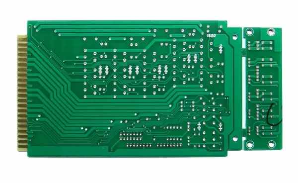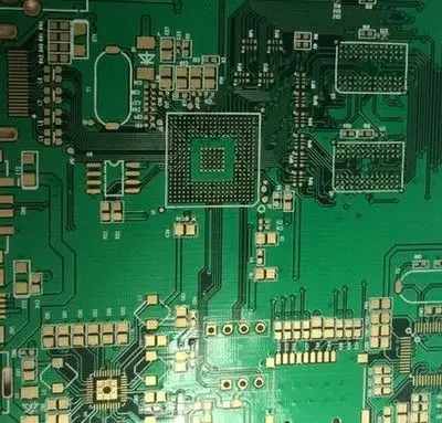
Pcb circuit board design, let's draw some parallel lines, convenience
Convenience should also be taken into account in the performance of printed circuit boards. The extra routing length is lossy. In addition, the signal will also attenuate on a longer route because there are more attack surfaces and the noise generator can be coupled to the signal. We must work within the available geometry, leaving us with countless choices.
Air gap and copper thickness are interrelated
This reminds me of other compromises that we must manage when designing PCB. First of all, the circuit board with large current will benefit from the thick copper layer to handle the power supply. At the same time, we also like to use narrow routing and package them together to avoid the internal area of larger equipment.
Getting the right stack into a balanced action allows for some fine pitch connections as well as some high current applications. The design rule of this setting will allow for a smaller air gap on the signal layer, while other rules set a broader interval rule to power up.
These two things cannot be good neighbors, so we need other levels to act as obstacles. Adding layers will increase the cost, so we must make full use of the available layers. In some cases, the small spacing rule applies only to local areas. Once there are no connectors or processors, a more conservative set of rules will apply. Dialing during this process is a balancing act.

How are components placed?
We know that small size is preferred. That's where those highly integrated circuits come from. The "all-purpose" system on chip (SOC) will actually have hundreds of passive components, and perhaps dozens of other integrated circuits to actually create a system. Most of these additional circuits want to be as close to the SOC as possible.
All memory and high-speed links want to occupy a seat on the table. Sufficient power may be required to ensure the use of short special power management ICs or PMICs. Of course, any analog line should be short and straight, and should not exceed the scope of SOC. Why are these functions not on SOC at first?
It comes down to chip architecture. Compared with the nearly invisible transistor gates that make up most of the SOC space, the memory cells are very large. These things must be put in their own packaging, just because they are the manufacturers of design.
However, the area around computing devices is a hot commodity. I mean literally. The more space you can place around it, the better. Faced with the requirements of small size, such documents. We want the parts to be close to each other and separate at the same time.
All these competitive factors will lead to strategic clustering, usually through its voltage decomposition of things, and the secondary focus is on its routing. In the balance process of PCB assembly placement, we also considered thermal interference and electromagnetic interference. If we can further expand the content, we can increase test access. At the same time, it would be great if we could compress the entire circuit board to make room for larger batteries in smaller enclosures than last year's products.
Trade offs when wiring printed circuit boards
Therefore, routing is a function of layout, and layout is a function of several factors as described above. Some of these factors compete directly with each other. Even with the best simulation, it is difficult to predict the nuances of overlap. Perfection is out of reach, so what we are looking for is enough. If it runs reliably during the warranty period, we have finished the work.
Given a runway of sufficient length, theoretically we can use the perfect memory bus, which uses the smallest twists and turns and the smallest space, while maintaining the optimal spacing of all kinds of connections. The time budget can be set to a minimum allowable deviation. The problem is that time is almost always short, so we need all the range that the signal can handle.
It seems impossible to make everyone happy. Everyone, including not only the internal team, but also each supplier, provides a reference design built around their chips, as if it would become the only thing on the board. The Circuit board assembly and the circuit board processing manufacturer explain the circuit board design and draw some parallel lines. In terms of performance, convenience should also be taken into consideration. The extra length of the wiring is wasted.


