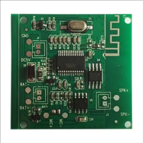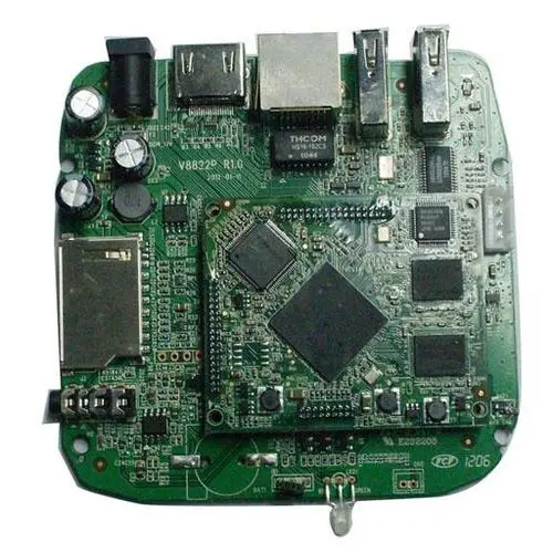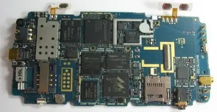
The quality of the design directly affects the performance of the circuit board. The design version is also very particular, especially the high frequency board. Here we summarize some high frequency board design skills to understand if necessary.
1. Improve PCB design specifications for high-precision etching. Consider that the total error of the specified line width is+/-0.0007 inches, manage the undercut and cross section of the wiring shape, and specify the electroplating conditions of the wiring sidewall. The overall management of wiring (wire) geometry and coating surface is very important for solving the skin effect problems related to microwave frequency and realizing these specifications, as well as for the design of high-frequency circuit boards.
2. Abundant grounding layers shall be provided. Moulded holes shall be used to connect these grounding layers to prevent the influence of 3D electromagnetic field on high-frequency circuit boards.
3. 45 ° angle shall be adopted for transmission line corner to reduce return loss.

4. The non electrolytic nickel plating or gold immersion plating process shall be selected, and the HASL method shall not be used for electroplating. The electroplating surface can provide better skin effect for the current of high-frequency circuit board. In addition, this highly weldable coating requires fewer leads, which helps reduce environmental pollution
5. There is tap inductance in the protruding lead, so avoid using components with leads. In high-frequency environments, surface mount components are preferred.
High frequency board
6. For signal vias, avoid using the via machining (PTH) process on the sensitive plate, because this process will cause lead inductance at the vias.
High frequency PCB design process
The rationality of high frequency PCB routing directly affects the performance of the circuit. In the design of high-frequency PCB circuit (especially for frequencies above 10MHz), the following points must be paid attention to in order to obtain the due high-frequency board characteristics:
1. Inductive component generated by wiring.
2. High frequency coupling between circuits.
3. High frequency impedance value of the ground.
1、 The inductance component generated by wiring shall be reduced as much as possible
In the design of High Frequency Circuit Board, the wiring connecting each component has inductance component. The longer the wiring is, the higher the electrical inductance component will be, which will deteriorate the frequency characteristics (low pass filter formed by inductance component and stray capacitance), and may also cause oscillation (phase deviation due to inductance component).
Therefore, in principle, the wiring should be short and thick, and the Layout of components should follow this principle. The terminals of pin transistor, resistor, capacitor and other components have inductance components, which cannot be ignored when the frequency is very high. Therefore, the terminals of components should also be as short as possible. It is better to use SMT chip components in high-frequency circuits to reduce the inductance of component terminals.
High frequency pcb board
Arrange Cl (decoupling capacitance of power supply) as close as possible to the load resistance (330 Ω). C2 is the emitter bypass capacitor, which should also be installed near the emitter of the transistor as far as possible.
2、 The high-frequency impedance value of the ground shall be reduced as much as possible
In low-frequency circuit, one point grounding is often used to make all grounding points have the same potential. In the high-frequency circuit board, the potential of each grounding point of the circuit must also be the same.
However, in the design of high-frequency circuit boards, it is often difficult to achieve one point grounding due to the long routing. Therefore, it is very important to reduce the impedance value of the ground so that the potential of each grounding point is as same as possible.
3、 Prevent high frequency coupling between circuits
The higher the signal frequency and the shorter the filter length, the easier it will become an electromagnetic wave and be launched into the air. Therefore, for signals on tens of MHz, most of the circuits should be isolated by copper or tinned iron sheets to prevent the coupling of internal and external high frequencies of PCB circuits. In the same circuit, in order to prevent the coupling inside the circuit, isolation can also be used, and the isolation cover can be grounded, which can also reduce the grounding impedance. In addition, inductors or magnetic rings are connected in series on the power supply line, and through capacitors can be added to prevent high-frequency coupling through the power line.


