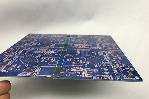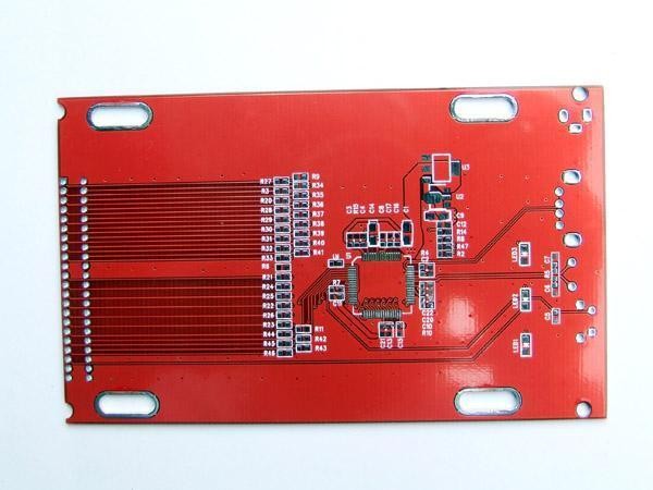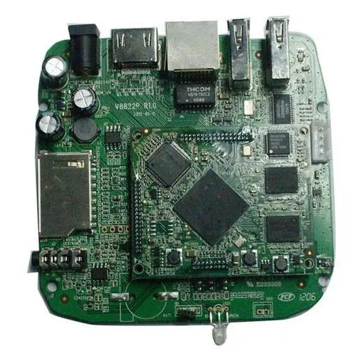
In fact, each electronic product is composed of one or more printed circuit boards (PCBs). The PCB fixes the IC and other components and realizes the interconnection between them. A large number of pcbs have been created for portable electronic devices, computers and entertainment devices. They are also used for testing equipment, manufacturing and spacecraft. Finally, almost every EE must design a pcb, which is not something that is taught in schools. However, engineers, technicians and even novice pcb designers can create high-quality PCB designs for any purpose and are confident that the results will meet or exceed the goals. Similarly, these designs can be completed on schedule and within budget while meeting design requirements. Designers need to consider the necessary documentation, pcb design steps and strategies, and final checks.
Basic design process
The ideal pcb design starts from the requirement analysis and continues to the final delivery. After getting the project, it is necessary to determine the pcb requirement analysis, which includes the designed functions, the functions that the pcb must have and perform, the interconnection with other circuits, the layout and the approximate final size. The ambient temperature range and issues related to the working environment shall be addressed and used to designate the material selected for the pcb. When selecting components and pcb materials, attention shall be paid to all foreseeable and potential threats to ensure that pcb can work normally during its service life. The circuit schematic diagram is drawn according to the schematic diagram. This detailed diagram shows the electrical implementation of each function of the pcb. After the schematic diagram is drawn, the final pcb layout should be completed and the area should be specified for the schematic block of each circuit.
Pcb design process
Bill of Materials
A bill of materials (BOM) should be generated at the same time as the schematic is created. While considering the tolerance standard, the components in the circuit shall be selected by analyzing the limiting operating voltage and current level of each node of the circuit. After selecting components that are electrically satisfactory, each component should be reconsidered based on availability, budget and size. The BOM must always be synchronized with the schematic. The BOM requires the quantity, reference code, value (ohm, farad, etc.), manufacturer's part number and pcb floor area of each component. These five requirements are critical because they define how much each part needs, explain the identification and circuit location while accurately describing each circuit element used for purchase and replacement, and explain the size of each part used for area estimation. It should be a concise list describing each circuit element, and too much information may make the development and management of the library too complex.
Pcb file
The pcb file shall include hardware dimension drawing, schematic diagram, BOM, layout file, component placement file, assembly drawing and description, and Gerber file set. Gerber fileset is a pcb term used by pcb manufacturers to create pcb layout output files. The complete Gerber file includes the output files generated from the circuit board layout file: silk screen up and down, top and bottom of solder mask layer, all metal layers, solder paste top and bottom, component diagram (XY coordinates), top and bottom of assembly drawing, drilling file, hole turning diagram, FAB outline (size, special functions), and grid file. The special functions included in the FAB contour include but are not limited to: notch, notch, bevel, backfill pad (for BGA type IC package, there are multiple pins under it), blind hole/buried hole through-hole, surface finish and leveling, hole tolerance, layers, etc.

Schematic Details
The schematics control the project, so accuracy and completeness are critical to success. They include information necessary for the correct operation of the circuit. The schematic diagram shall include sufficient design details, such as pin numbers, names, component values and ratings.
Each schematic symbol has a manufacturer's part number that determines price and specification. The package specification determines the package size of each component. In the first step, according to the available area and welding method, ensure that the bare copper of each pin is placed in the correct position and slightly larger than the assembly pin (3 to 20mil). When designing pcb packaging, please consider assembly and follow the manufacturer's recommended pcb packaging. Some components are micro encapsulated, so there is no excess copper allowance. Even in these cases, a 2.5 to 3mil electrode should be applied between each pin on the plate. Follow the rule of 10. The final hole diameter of the small through hole is 10mil, and there is also 10mil pad ring. The wiring shall be 10mil or more away from the edge of the plate. The wire spacing is 10mil (5mil air gap, 5mil wire width, 1oz copper). Through holes with a diameter of 40 mils or more shall be provided with pad rings to improve reliability. For the outer copper plane from the plane to the pin, an additional clearance of 15 to 25 mils beyond the design rules shall be set. This reduces the risk of bridging on all solder joints.
Component placement
The next step is to place the components and locate them based on thermal management, functional and electrical noise factors. After assigning the contour and interconnection position of the component, the first component placement step starts. Immediately after placing each component, a placement review should be conducted and adjustments made to facilitate cabling and optimize performance. The layout and packaging dimensions are usually reconsidered and changed at this time based on size and cost. Components that absorb more than 10 mW or conduct more than 10 mA of current shall be considered powerful enough to take into account other thermal and electrical factors. Sensitive signals shall be isolated from the noise source through a plane and the impedance shall be controlled. The power management component shall utilize the ground plane or power plane for heat flow. Make high current connections according to an acceptable connection voltage drop. For layer conversion of high current path, two to four through holes shall be used at each layer conversion, and multiple through holes shall be placed at the layer conversion to improve reliability, reduce resistance and inductance loss and improve thermal conductivity.
Heat dissipation problem
The heat generated by the IC is transferred from the device to the copper layer of the pcb. The ideal thermal design will make the temperature of the whole circuit board the same. The thickness, number of layers, continuity of thermal path and circuit board area of copper will directly affect the working temperature of components.
Pcb design heat dissipation
To reduce the operating temperature easily, use a solid ground or power layer with multiple layers directly connected to the heat source with multiple vias. Effective heat conduction can make the heat evenly distributed from the heat source to the entire PCB board, thus significantly reducing the temperature.
Pcb heat conduction
(Effective heat conduction can make the heat evenly distributed from the heat source to the PCB surface)
In the case of uniform heat distribution, the following formula can be used to estimate the surface temperature:
P=(thermal convection) x area x( Δ T)
Explain:
P=Power consumption on the board
Area=circuit board (X axis x Y axis)
Δ T=surface temperature – ambient temperature
Thermal convection=convection constant based on environmental conditions
Trimmer placement
The elements shall be arranged in the following order: connector, power circuit, sensitive circuit and precision circuit, key circuit elements, and then arranged in sequence. The schematic diagram is built around each part of the pcb and is fully interconnected. The routing priority of the circuit is selected according to the power level, noise sensitivity or generation and routing capability.
Generally, the wiring width is 10 to 20 mils, which is used to carry 10 to 20 mA wiring, and the wiring width is 5 to 8 mil, which is used to carry less than 10 mA current. When wiring with high impedance nodes, high frequency (greater than 3 MHz) and fast changing signals should be carefully considered.
The designer should check the layout and should iteratively adjust the physical location and wiring path until the circuit is optimized for all design constraints. The number of layers depends on the power level and complexity. Pairs of layers are added because the copper cladding is made in this way. Power signal and plane wiring, grounding scheme and the ability of the circuit board to be used as expected will affect the operation.
The final inspection shall include verifying whether the sensitive nodes and circuits have correctly shielded the noise source, whether there is a solder mask between the pin and the via, and whether the silk screen is clear and concise. When determining layer stacking, use the first inner layer below the component side as the ground and assign the power plane to other layers. The stack is created in such a way that the board is balanced relative to the midpoint of the Z axis.
Consider any problems encountered by the pcb designer in the review process, and correct the pcb according to the feedback generated by the review. The change list is created and validated during each audit iteration until the board is finalized. Use the Design Rule Checker (DRC) to keep the design error free during all phases of the layout. DRC can only capture errors that have been programmed to monitor, and DRC rule sets usually change based on individual designs. At least, the design rule check should cover the spacing between packages, unconnected networks (identify the name of each node in the circuit), short circuited networks, whether there is an air gap, if vias are too close to the pad, if vias are too close to each other, and violate the vertical gap.
Many other important DRC rules can be set to ensure robust design and should be studied and understood. For example, maintain a clearance of 5mil or more. Through holes shall not be located in surface mount pads (unless backfilled). In addition, the welding resistance layer shall be located between all welding points.
Cost is usually the driving factor behind pcb design, so it is necessary to understand the cost increasing factors in pcb manufacturing. The typical pcb board has two to four layers, no drill hole with diameter less than 10mil, and the minimum air gap and routing width are 5mil. The thickness of standard FR-4 should also be 0.062 inch and the weight of copper foil should be 1 ounce. Additional layers, extra thick or thin plates, vias in pads, backfilled vias (preferably non-conductive due to conductivity limitations and thermal expansion differences), blind holes/buried holes, and delivery times all increase the total cost.
At the beginning of pcb design, the manufacturer's capabilities should be understood. When designing a manufacturability pcb, the IC company is usually contacted regularly on functions and cost reduction technologies.
summary
pcb design may be very complex, but through some skills and practice, we can design high-quality circuit boards.


