Circuit board factory introduces the wiring skills of multi-layer PCB
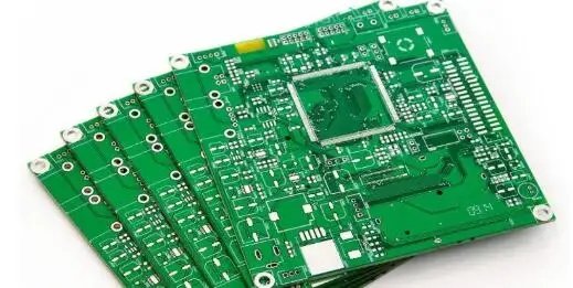
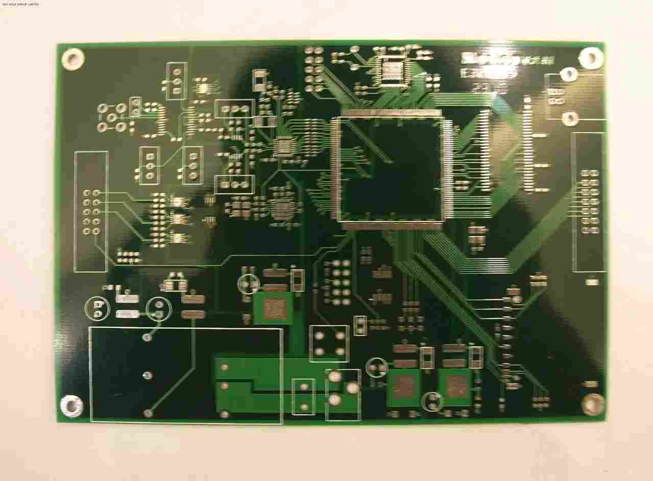
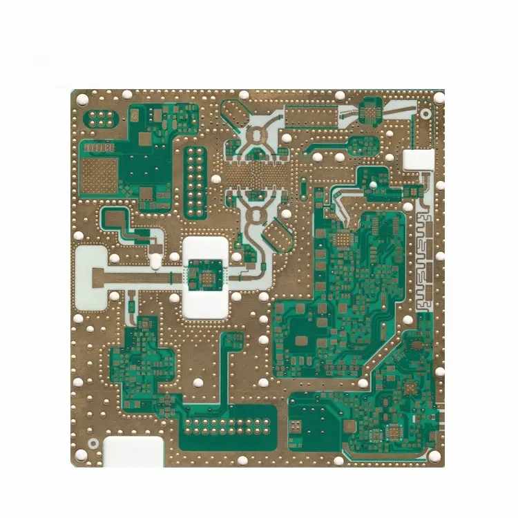
The design of printed circuit board is based on the circuit schematic diagram to realize the functions required by the circuit designer. The design of printed circuit board mainly refers to layout design, which needs to consider the layout of external connections. The optimal layout of internal electronic components, the optimal layout of metal wiring and through-hole, electromagnetic protection, heat dissipation and other factors. Excellent layout design can save production costs and achieve good circuit performance and heat dissipation. Simple layout design can be realized by hand, while complex layout design needs to be realized by computer aided design (CAD)
1. The wiring shall be straight line or 45 degree broken line to avoid electromagnetic radiation.
2. The lines between different layers should not be parallel as far as possible to avoid the formation of actual capacitance.
3. For wiring above 3 points, try to let the line pass through each point in turn to facilitate testing, and the line length should be as short as possible.
4. Try not to pay off wires between pins, especially between and around integrated circuit pins
5. Ground wire and power wire shall be at least 10-15mil (for logic circuit).
6. Try to connect the grounding wires together to increase the grounding area. The lines shall be as neat as possible.
7. The structure shall be considered for element emission. The positive and negative electrodes of SMD elements shall be marked at the end of package to avoid space conflict.

8. Pay attention to the uniform arrangement of elements for installation, plug-in and welding operations. The text shall be arranged in the current character layer in a reasonable position, and the orientation shall be paid attention to to avoid being blocked, so as to facilitate production.
9. The components of the function block shall be placed together as much as possible, and the components near the LCD such as zebra stripes shall not be too close.
10. It is better not to place pads, too empty, etc. under the battery holder, and the PAD and VIL dimensions are reasonable
11. At present, the printed board can be used for 4? 5 mil wiring, but usually 6 mil line width, 8 mil line spacing, 12/20 mil bonding pad. The wiring shall consider the influence of the injected current, etc.
12. After wiring, carefully check whether each connection line (including NETLABLE) is really connected (lighting method can be used).
13. The oscillating circuit components shall be as close to the IC as possible, and the oscillating circuit shall be as far away from the antenna and other vulnerable areas as possible. The grounding pad shall be placed under the crystal oscillator.
14. Various methods, such as reinforcement and hollow element placement, shall be considered to avoid excessive radiation sources.
15. The vias shall be coated with green oil (set to a negative value).
16. PCB design process: A: design schematic; B: Confirm the principle; C: Check whether the electrical connection is complete; D: Check whether all components are encapsulated and the dimensions are correct; E: Place components; F: Check whether the component position is reasonable (1:1 diagram can be printed for comparison); G: The ground wire and power line can be laid first; H: Check whether there are flying lines (other layers except the flying line layer can be turned off); 1: Optimize wiring; J: Check the wiring integrity again; K: Compare the network table and check whether there is any omission; 50: Check whether there are wrong labels in the rule verification; M: Text description sorting; N: Add board making logo text description; O: Comprehensive inspection. PCB Assembly and PCB processing manufacturers explain the introduction of multi-layer PCB wiring skills.


