electromagnetic compatibility Design of Printed Circuit Board Design of Power Supply
Electromagnetic compatibility refers to the ability of equipment or system to work normally in its electromagnetic environment without unbearable electromagnetic interference to anything in the environment. The purpose of EMC design is to make electronic equipment not only suppress various external interference, make electronic equipment work normally in a specific electromagnetic environment, but also reduce the electromagnetic interference of electronic equipment itself to other electronic equipment. As the sensitivity of electronic equipment becomes higher and higher, the ability to accept weak signals becomes stronger and stronger, the frequency band of electronic products becomes wider and wider, and the size becomes smaller and smaller, so the anti-interference ability of electronic equipment is required to be stronger and stronger. The electromagnetic wave generated by some electronic equipment during operation is easy to form electromagnetic interference to other electronic equipment around, causing faults or affecting signal transmission. In addition, excessive electromagnetic interference will form electromagnetic pollution, endanger people's health and damage the ecological environment. This paper analyzes several key EMC technologies in PCB design.

1 Design of power supply
The power supply of electronic equipment is widely connected with other functional units. On the one hand, the useless signals generated in the power supply will be easily coupled to each functional unit; on the other hand, the useless signals in one unit may be coupled to other units through the common impedance of the power supply. Therefore, the following measures should be taken in the power supply design.
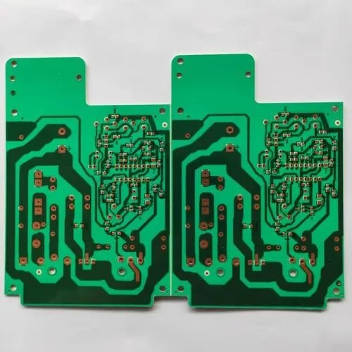
(1) According to the current of the printed circuit board, the width of the power line should be thickened as much as possible to reduce the loop resistance, so that the direction of the power line and ground wire is consistent with the direction of data transmission; At the same time, the power layer and layer are used in the multilayer PCB to reduce the line length from the power line to the power layer or layer. This helps to enhance the anti noise ability;
(2) If possible, make the power supply supply separate for each functional unit, and all circuits using the public power supply as close to each other as possible and compatible with each other;
(3) The power filter is used on the AC and DC trunk lines to prevent external interference from entering the equipment through the power supply, to prevent switching transients and other signals generated inside the equipment from entering the primary power supply, and to effectively isolate the input and output lines of the power supply and the input and output lines of the filter;
(4) The power supply shall be effectively shielded from electromagnetic field, and the high-voltage power supply shall be isolated from the sensitive circuit as far as possible, especially the switching power supply, which will cause high-frequency radiation and conduction disturbance. The electrostatic shielded power transformer shall be used to suppress the common mode interference on the power line. The multiple shielded isolation transformer has better performance;
(5) The power supply in all circuit functional states shall maintain low output impedance. Even in the RF range, the output capacitor shall also exhibit low impedance, and the regulator shall have fast enough response time to suppress high-frequency ripple and transient loading;
(6) Rectifier diode shall work at the lowest current density to provide sufficient RF bypass for regulator diode;
(7) The power transformer shall be symmetrical and balanced rather than power balanced transformer. The lower limit of saturation magnetic induction (Bm) shall be taken as the core material used. No matter under any circumstances, it must be ensured that the iron core is not driven to the saturation state. The iron core structure of the transformer shall preferably be Type D and Type C, followed by Type E. The circuit board factory explains and analyzes several key technologies of electromagnetic compatibility in PCB PCB design.


