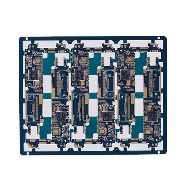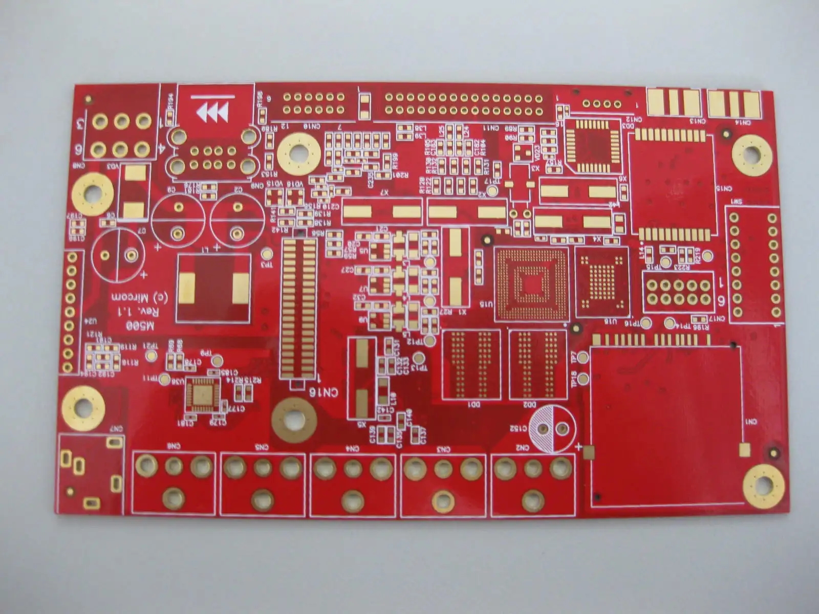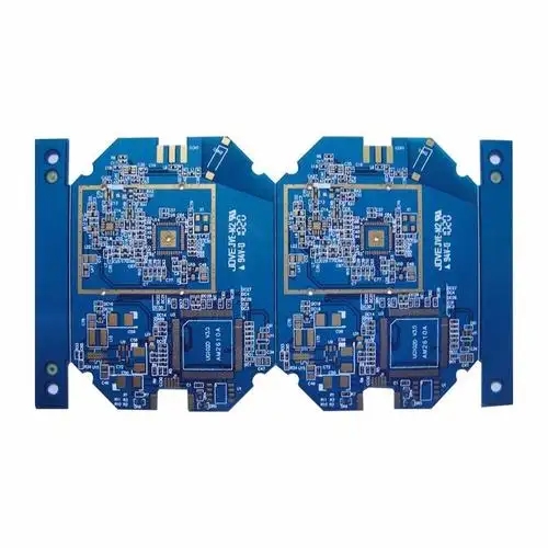
Explanation of solutions to various problems in pcb circuit board design
In the design process of Printed Circuit Board (PCB), many different methods can be adopted to solve various problems. The adjustment of the existing design scheme itself, such as adjusting the line layout to reduce noise; There are also methods for PCB layout. The design components can be automatically installed through the layout tool, but if the automatic layout can be manually adjusted, it will help to improve the quality of the circuit board design. Through this measure, design rule detection will rely on technical documents to ensure that the design of the circuit board can meet the requirements of the circuit board manufacturer.
Separating different circuit board layers can reduce the associated capacitance. However, this will increase the number of circuit board layers, which will increase the cost and bring more through-hole problems. Although the use of orthogonal grid power supply system and grounding circuit design may increase the physical size of the circuit board, it can effectively play the role of the grounding layer in the double-layer circuit board and reduce the capacitance and the complexity of circuit board production.

Design tools, including DesignSpark PCB, can help engineering designers solve many problems at the beginning of design, but engineering designers still need to have a full understanding of the design requirements of printed circuit boards (PCBs). For example, if the editor of a printed circuit board (PCB) needs to know the number of layers of the PCB at the beginning of the design, for example, a double-layer circuit board needs to have a ground plane and a power supply plane, and two mutually independent board layers. Automatic component layout technology is very useful. It can help designers spend more time to design the layout area of equipment. For example, if the power supply equipment is too close to sensitive signal lines or areas with high temperature, many problems will arise. Similarly, signal lines can also be automatically routed to avoid most problems. However, analysis and manual operation of high-risk areas will help greatly improve the quality of PCB design, increase revenue and reduce overall cost.
Design rule detection is also a very powerful tool, which can detect lines to ensure that the distance between lines is not too close, resulting in too short loops. However, the overall design still has high economic value. The design planning detection tool can also be used to detect and adjust the power layer and ground plane to avoid large associated capacitance area.
The above tools will also be of great help to Gerber and Excelton in their work on circuit and circuit board printing, through hole drilling and other aspects in order to produce the final design product. In this way, the technical documents are closely linked with the circuit board manufacturer.
PCB processing, PCB Assembly, PCB design, PCBA processing manufacturers will explain solutions to various problems in PCB design.
conclusion
Many problems need to be considered in the design process of printed circuit board (PCB), and tools including DesignSpark PCB can effectively handle most of these problems. By adopting some best practice guidelines, engineering designers can effectively reduce costs, improve the reliability of the circuit board, meet the requirements of the system specification, and deflect the system certification at a lower cost, thus avoiding more problems.


