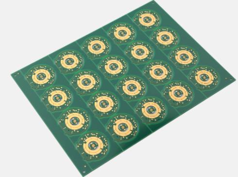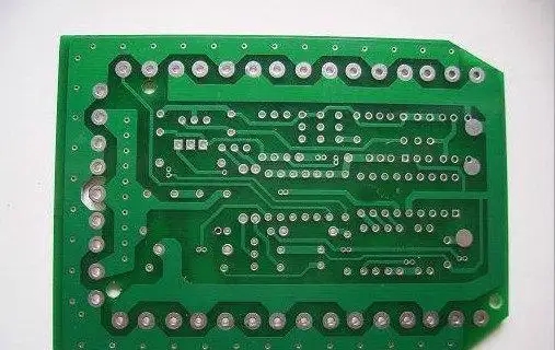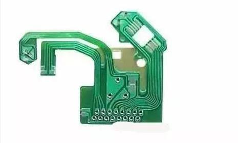
The design of printed circuit board is based on the circuit schematic diagram to realize the functions required by the circuit designer. The design of printed circuit board mainly refers to layout design, which needs to consider the layout of external connections. The optimal layout of internal electronic components, the optimal layout of metal wiring and through-hole, electromagnetic protection, heat dissipation and other factors. Excellent layout design can save production costs and achieve good circuit performance and heat dissipation. Simple layout design can be realized by hand, while complex layout design needs to be realized by computer aided design (CAD)
1. CLK (including DDR-CLK)
Basic routing requirements:
1. The clk part shall not cross other lines, and the Via shall not exceed two
2. No cross cutting is allowed, and no threading is allowed between two pads of parts
3. The front side of Crystal shall not cross the line, and the reverse side shall not cross the line as much as possible
4. The minimum spacing shall be used for parallel routing of Differential Pair
5 The distance between clk and high-speed signal line (1394, usb, etc.) shall be more than 50mil

2. VGA:
Basic routing requirements:
1. RED, GREEN and BLUE must be wound together, and GND shall be included as appropriate R. G. B Do not cut across.
2 HSYNC and VSYNC must be wound together, and GND shall be included as appropriate
3. LAN:
Basic routing requirements
1. The same group of wires must be wound together.
2 Net: RX, TX: different pair winding is required
4.1394:
Basic routing requirements:
1. Different pair winding, same layer, parallel, do not cut across
2. The same group of wires must be wound together.
3. The distance from high-speed signal line shall not be less than 50mil
5. USB:
Basic routing requirements:
1 Different pair winding, same layer, parallel, do not cut across
2 The same group of wires must be wound together
6. CPU-NB (AGTL):
Basic routing requirements:
1. The same group and the same layer or the same group and different layers shall be wired together
2. When winding, the same NET spacing shall not be less than four times the line width
3. NET length shall be added to the package length of CPU&NB
4. STB N/P (+/-) Differential Pair winding
5 VIA type is VIA26
7. CPU-SB:
Basic routing requirements:
1. The same group of wires must be wound together
2 pull up resistance, which must be close to CPU
8. NB-DDR:
Basic routing requirements:
1. Damping resistance and terminal resistance (drain resistance) NET: MD&MA&DQS&DQM cannot be shared
2. The wires in the same group and on the same layer shall be wound at four times the spacing
9. NB-AGP:
Basic routing requirements:
1. The same group and the same layer or the same group and different layers shall be wired together
2. When winding, the same NET spacing shall not be less than four times the line width
3. STB+/- Differential Pair winding
4 In the constraint area, try to follow the guide lauout
10. NB-SB:
Basic routing requirements:
1 Walk together without crossing the cutting line
2. When winding, the same NET spacing shall not be less than four times the line width
11. IDE:
Basic routing requirements:
1. In the same group and layer, the winding wires must be wound together in the same group
2. When winding, the same NET spacing shall not be less than four times the line width
12. PCI:
Basic routing requirements:
At most three wires pass between 1PAD and PAD
2. The resistance and capacitance shall be placed neatly as far as possible
13. CNR:
Basic routing requirements:
1. Walk together
14. POWER:
Basic routing requirements:
1. Generally, 30: 5 wiring is used, the time interval is not less than 10 MIL when the line width is more than 40 MIL, and the VIA is VIA40, (or two VIA24 are printed)
15. OTHER:
Basic routing requirements:
1. All IO lines cannot cross layers.
2. COM1, COM2, PRINT (LPT), GAME go together with the group.
3 COM1 and COM2 go through the capacitor first and then pull out.
16. Additional test pilot:
1. The target of 100% should be at least 98%
2. The distance between pins to pins should be preferably 75 mils and at least 50 mil
3. The minimum pad of test point is 27mil, and 35mil shall be used as far as possible
4. The distance between the single side test point and the outer frame of the part on the same layer is greater than 50MIL
5. CPU socket includes ZERO pull rod, and top side test point cannot be placed inside
6. The front end of the clk does not need to add test points. The back end can replace via with test_ Via. (To be agreed by the customer)
7. The winding of different pairs shall not be affected.
17. Modify DRC:
1. Complete DRC check, internal check, and check of unconnected PIN
2. All nets shall not be short circuited. No redundant line segments are allowed
18. Copper foil coating:
For parts requiring copper foil coating, net shall be coated with copper foil correctly
19. Text placement:
1. The text shall be marked from left to right and from top to bottom in the same direction
2. Parts shall be marked as close as possible to the parts
3. Properly place the feet of parts and mark the polarity
4. Whether the part symbol is marked.
CN, JP: foot mark (pay attention to the direction).
Polarity of parts: ※ Capacitance: +※ Crystal: G, D, S ※ Diode: A, K5 Delete redundant lines and marks.
PCB processing, PCB Assembly, PCB design and PCBA processing manufacturers will explain the basic 19 rules of PCB layout in detail.


