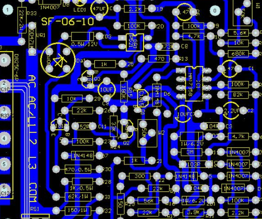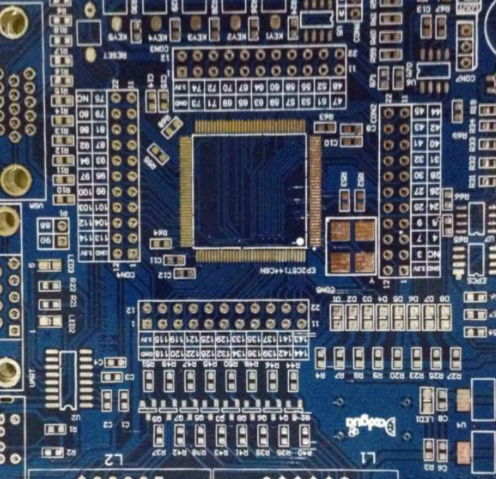
Description of PCB proofing parameter analysis steps
Generally, PCB boards produced need to be processed by the board manufacturer After proofreading, the technicians will weld the parts, and finally assemble it into the shell and package to form a complete product Then what related parameters and instructions need to be provided for PCB proofing?
[PCB proofreading description items]
Data: The first thing to explain is what kind of data PCB needs. At present, FR4 is the most common, and the main information is epoxy resin peeling fiber cloth board.
Board layer: Explain the number of layers for making PCB. (The price of PCB varies with the number of production layers, and the proofing process of PCB is similar.)
Color of solder mask: There are many colors, which can also be selected according to the company's requirements, generally green.
Silk screen color: The color of silk screen font and border on printed circuit board is usually white.
Copper thickness: Generally, the copper thickness is calculated scientifically according to the current of PCB circuit. Generally speaking, the thicker the better, but the higher the cost, which requires a reasonable balance.
Whether the vias are covered with solder mask: the solder mask is used to insulate the vias, otherwise it is used to make the vias uninsulated.
Surface coating: tin spraying and gold plating.
Quantity: The number of PCBs produced shall be clearly stated
What is PCB proofing? What does PCB proofing mean
What is PCB proofing
PCB proofing usually means that after the engineer completes PCB layout design, electronic products are sent to PCB manufacturers and processed into PCBs for trial production
The update and iteration of electronic products are relatively fast, and the demand for PCB proofing is growing gradually, and the market share is expanding. With the increasing technological requirements of electronic products, information becomes more and more high-speed, leading to the rise of multi-layer PCB proofing relatively fast.
What is the user group of PCB proofing
Mainly electronic engineers, but also academic research, research institutions and other student groups.
How to Select a Suitable PCB Proofing Manufacturer
Circuit board

Mainly focus on several links:
1. Select large companies and enterprises, with more stable relative strength and more standardized management.
2. Select enterprises around Shenzhen and leading enterprises of electronic products, with complete supporting facilities to ensure delivery.
3. Choose a company with good reputation, service focus and cultural theme.
PCB proofing process
1. Etching
Etching is the use of chemical reactions to etch the copper layer of non circuit parts.
2. Green oil
Green oil transfers the pattern of green oil film to the circuit board to protect the circuit and prevent tin on the circuit when soldering parts.
Process: Grinding plate printing, photosensitive green oil plate exposure; Grinding plate printing first side drying plate printing second side drying plate
3. Text
Characters are provided as tags for easy identification
Process: After finishing the green oil - cooling and standing - adjusting the screen printing characters - rear cubic
4. Gilded finger
Apply a nickel/gold layer of the required thickness on the finger of the plug to make it harder and more wear-resistant
Process flow: upper plate - degreasing - twice cleaning - micro etching - twice cleaning - pickling - copper plating - cleaning - nickel plating - cleaning - gold plating
2 Tinplate (parallel process)
Tin spraying is to spray a layer of lead tin on the bare copper surface that is not covered with the solder mask to protect the copper surface from corrosion and oxidation and ensure good welding efficiency.
Process flow: micro erosion - air drying - preheating - rosin coating - solder coating - hot air leveling - air cooling - cleaning and air drying
5. Forming
The method of forming the shape required by the customer through molding or CNC gongs. Organic gong, beer board, gong, hand cut
Note: The data precision of machine board and beer board is high. The hand gong is the second, and the smallest hand chopping board can only make some simple shapes.
6. Test
Through electronic 100% test, it can detect defects that affect the function, such as open circuit and short circuit that are not easy to be found visually.
Process: upper mold - remove template - test - pass - FQC visual inspection - unqualified - repair - return test - OK-REJ - scrap
7. Final inspection
Repair small defects by 100% visual inspection of plate appearance defects to avoid problems and defective plates from flowing out.
Specific workflow: incoming materials - viewing information - visual inspection - qualified - FQA spot check - qualified - packaging - unqualified - processing - qualified
The above is the explanation given by the editor of pcb circuit board company.
If you want to know more about PCBA, you can go to our company's home page to learn about it.
In addition, our company also sells various circuit boards,
High Frequency Circuit Board and SMT chip are waiting for your presence again.


