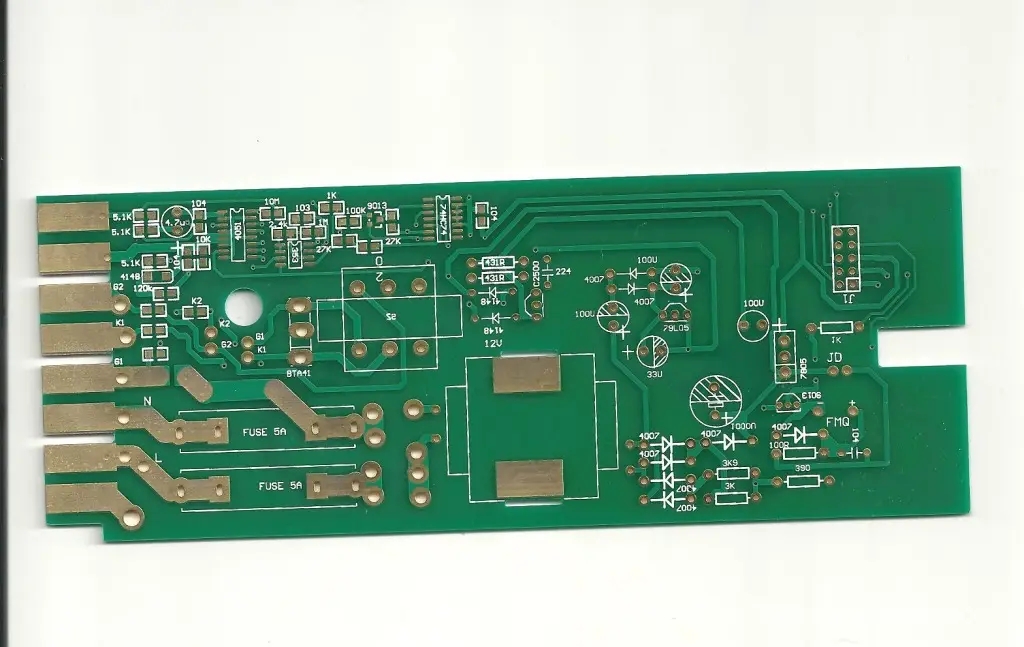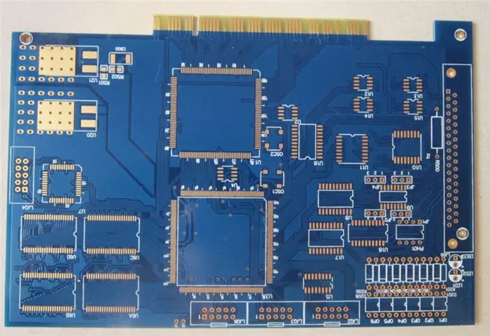
PCB manufacturers explain the use of parameter constraints for PCB design
PCB manufacturers, PCB designers, PCBA manufacturers explain to you that PCB manufacturers use parameter constraints to design PCB
Nowadays, the factors considered in pcb design are more and more complex, such as clock, crosstalk, impedance, detection, manufacturing process and so on. The parameter constraint editor can incorporate these parameters into formulas, helping designers better handle these sometimes contradictory parameters in the design and production process.
In recent years, the requirements for pcb layout and routing are becoming more and more complex. The number of transistors in integrated circuits is still rising at the speed predicted by the Moore's Law, which makes the device speed faster and the rise time of each pulse shorter. At the same time, the number of pins is also increasing - often up to 500 to 2000 pins. All of these will bring the problems of density, clock and crosstalk when designing pcb.
A few years ago, most pcbs had only a few "critical" nodes (net), which usually meant that they were constrained in impedance, length and gap. pcb designers generally first manually route these lines, and then use software to automatically route the entire circuit on a large scale. Today's pcb often have 5000 or more nodes, and more than 50% of them are critical nodes. Due to the pressure of time to market, it is impossible to use manual wiring at this time. In addition, not only the number of critical nodes has increased, but also the constraints of each node are increasing.
These constraints are mainly caused by the increasing complexity of parameter correlation and design requirements. For example, the interval between two routing lines may depend on a function related to node voltage and PCB materials. The reduction of digital IC rise time will have an impact on the design of both high clock speed and low clock speed. Because the pulse generation is faster, the establishment and retention time will be shorter, In addition, interconnection delay, as an important part of the total delay of high-speed circuit design, is also very important for low-speed design.
If the circuit board can be designed larger, some of the above problems will be easier to solve, but the current development trend is just the opposite. Due to the requirements of interconnect delay and high-density packaging, the circuit board is becoming smaller and smaller, which leads to high-density circuit design. At the same time, miniaturization design rules must be followed. With the reduction of rise time and these miniaturization design rules, the crosstalk noise problem becomes more and more prominent, while the spherical grid array and other high-density packages themselves will also aggravate crosstalk, switching noise and ground wire bounce.
Limitations of fixed constraints
The traditional way to deal with these problems is to convert electrical and technological requirements into fixed constraint parameters based on experience, default values, tables or calculation methods. For example, engineers may first determine a rated impedance when designing circuits, and then "estimate" a rated linewidth that can reach the required impedance according to the final process requirements, or use calculation tables or arithmetic programs to test the interference, and then calculate the length constraints.
This method usually needs to design a set of empirical data as the basic guiding principle for pcb designers, so that they can use these data when designing with automatic placement and routing tools. The problem with this method is that empirical data is only a general principle. In most cases, they are correct, but sometimes they do not work or lead to wrong results.
Let's take the example of impedance determination above to see the possible error caused by this method. Factors related to impedance include dielectric properties of circuit board materials, copper foil height, distance between each layer and ground/power supply layer and line width. Since the first three parameters are generally determined by production process, designers usually control impedance by line width. Since the distance from each line layer to the ground or power supply layer is different, it is obviously wrong to use the same empirical data for each layer. In addition, the production process or circuit board characteristics used in the development process may change at any time, so the problem will be more complex.
Most of the time, these problems will be exposed in the prototype production stage, and they are generally solved by repairing the circuit board or redesigning the board after finding out the problems. The cost is relatively high, and the repair often brings additional problems that require further debugging. Finally, the revenue loss caused by delayed time to market is much higher than the debugging cost. Almost every electronic manufacturer is faced with such a problem, which ultimately comes down to the fact that the traditional PCB design software cannot keep up with the current requirements for electrical performance, which is not as simple as the empirical data of mechanical design.
Solutions: parametric constraints
At present, design software suppliers try to solve this problem by adding parameters to constraints. The most advanced part of this method is that it can detail the mechanical indicators that fully reflect various internal electrical characteristics. as long as it is added to the pcb design, the design software can use this information to control the automatic placement and routing tool.

When the subsequent production process changes, there is no need to redesign. The designer can automatically change the relevant constraints by simply updating the process characteristic parameters. The designer can then run DRC (Design Rule Check) to determine whether the new process violates other design rules, and find out which aspects of the design should be changed to correct all errors.
Constraints can be input in the form of mathematical expressions, including constants, various operators, vectors and other design constraints, providing a parametric rule driven system for designers. Constraints can even be input in the form of table lookup, and stored in the design file of pcb or schematic diagram. The pcb wiring, copper foil area location and layout tools shall comply with the constraint rules generated by these conditions. DRC verifies whether the entire design conforms to these constraints, including line width, spacing and space requirements (such as area and height restrictions).
A very simple example is the rise time constraint, which is generally set as a constant of 1.5ns. According to this condition, the constraint of the maximum routing length can be obtained, that is, 5800ml/ns is multiplied by the rise time of 1.5ns. A slightly more complex example is element spacing, which is determined by multiplying the tangent value of the detection angle by the device height. This formula can calculate the minimum element spacing value.
Hierarchical management
One of the main advantages of parametric constraints is that they can be handled hierarchically. For example, the global line width rule can be used as a design constraint in the whole design. Of course, there will be individual regions or nodes that cannot follow this principle. In this case, you can bypass the higher-level constraint and adopt the lower level constraint in hierarchical design. Taking the Parameter Constraint Solver, the constraint editor of ACCEL Technologies, as an example, there are seven levels of constraints:
1. Design constraints are used for all objects without other constraints.
2. Hierarchical constraint, used for objects on a layer.
3. Node type constraint, used for all nodes included in a type.
4. Node constraint, used for a node.
5. Inter class constraint refers to the constraint between two types of nodes.
6. Space constraint, used for all devices in a space.
7. Device constraint, used for a device.
The software follows each design constraint in the order from individual devices to the whole design rules, and displays the application order of these rules in the design in a graphical way.
·Example 1: Line width=f (impedance, layer spacing, dielectric constant, copper foil height)
Here an example is given to illustrate how parametric constraints can be used as design rules to control impedance. As mentioned above, impedance is a function of dielectric constant, distance to the nearest line layer, copper wire width and height. Since the impedance required by the design has been determined, the impedance formula can be rewritten by taking these four parameters as relevant variables at will. In most cases, only the line width is the parameter that the designer can control.
Because of this, the restriction on line width is a function of impedance, dielectric constant, distance to the nearest line layer and copper foil height. If the formula is defined as a hierarchical constraint and the manufacturing process parameters are defined as a design level constraint, the software will automatically adjust the line width to compensate when the designed line layer changes. Similarly, if the designed PCB is produced by another process and the copper foil height changes, the relevant rules in the level can be automatically recalculated by changing the copper foil height parameter in the design level.
·Example 2: Device interval=max (default interval, f (device height, detection angle))
The obvious advantage of using parameter constraints and design rule checking at the same time is that when the design is modified, the parameterization method has good portability and monitoring. This example shows how to determine the device spacing according to the process characteristics and test requirements. The above formula indicates that the device spacing is a function of device height and detection angle.
Generally, the detection angle is a constant for the whole board, so it can be defined at the design level. When testing is performed by different machines, the entire design can be updated by simply entering new values in the design level. After the performance parameters of the new machine are input, the designer can know whether the design is feasible by simply running the DRC to check whether the device spacing conflicts with the new interval value, which is much easier than analyzing first, then correcting, and then hard calculating according to the new interval requirements.
·Example 3: Component layout
In addition to organizing design objects and constraints, design rules can also be used for component layout, that is, it can detect where to place components according to constraints without causing errors. The highlighted part in Figure 1 is the device placement area meeting the physical constraints (such as the spacing with the board edge and the device spacing), and the highlighted part is the device placement area meeting the electrical constraints (such as the maximum routing length). Only the area meeting the spatial constraints is displayed. Finally, Figure 4 is the intersection of the parts in the first three figures, which is the effective layout area. The devices placed in this area can meet all constraints.
In fact, it can greatly improve its maintainability and reusability to generate constraints in a modular way. New expressions can be generated by referring to the constraint parameters of different layers in the previous stage. For example, the line width of the top layer depends on the distance and copper wire height of the top layer and the variables Temp and Diesel in the design level_ Const。 Please note that the design rules are displayed from low to high. Changing a higher constraint will immediately affect all expressions referencing this constraint.
Design reuse and documentation
Parametric constraints can not only significantly improve the initial design process, but also be more useful for engineering change and design reuse. Constraints can be used as part of the design, system and documentation. If they are not stored in the minds of engineers or designers, they may slowly forget when they move to other projects. The constraint document records the electrical performance rules that should be followed in the design process, so that others have the opportunity to understand the designer's intent, so that it is easy to apply these rules to new manufacturing processes or change them according to electrical performance requirements. Later reusers can also know the accurate design rules and change them by entering new process requirements, without having to guess how to get the line width.
Conclusion
The parameter constraint editor is helpful for pcb layout and routing under multi-dimensional constraints. It is also the first time that the automatic routing software and design rules are checked completely according to complex electrical and technological requirements, rather than just relying on experience or simple and useless design rules. The result is that the design can be successful once, reducing or even canceling the prototype debugging. PCB manufacturers, PCB designers, and PCBA manufacturers explain to you that PCB manufacturers use parameter constraints to design PCBs.


