Avoid using power filter errors in PCB electronic devices
In the process of experimental testing, we often encounter such a situation: although the PCB design engineer has connected the power filter to the equipment power line, the equipment still cannot pass the "conducted disturbance voltage emission" test The engineer thinks that the filtering effect of the screening program is not good Repeated replacement of the screening program still fails to achieve the desired effect
The analysis of PCB equipment exceeding the standard involves the following two aspects:
1. The disturbance generated by the device is too strong
2. Insufficient equipment filtration
For the first case, we can take measures at the interference source to reduce the interference intensity, or add the order of the power filter to improve the filter's ability to suppress interference. For the second case, besides the poor performance of the filter itself, the installation method of the filter also has a great impact on its performance. This is often overlooked by design engineers.
In many tests, we can make the equipment pass the test successfully by changing the installation method of the screening program. The following are some examples of how common filter installation methods affect filter performance.
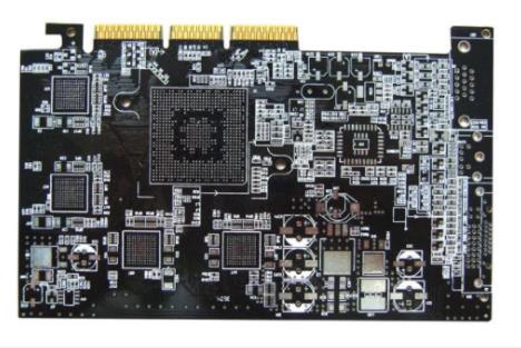
Circuit board

Input line is too long
After entering the main chassis, the power cord of many PCB devices will pass through a long wire and then be connected to the input end of the filter. For example, the power cord is input from the back panel of the main chassis, transmitted to the power switch on the front panel, and then returned to the back panel to connect to the filter. Or the installation position of the screening program is far away from the power cord inlet, which causes the lead to be too long.
Because the lead from the power supply inlet to the filter input is too long, the electromagnetic interference generated by the equipment is recoupled to the power line through capacitive or inductive coupling. The higher the frequency of the interference signal, the stronger the coupling, leading to experimental failure.
Flat pedestrian line
In order to make the wiring in the host shell beautiful, some PCB engineers often bundle the cables together, which is not allowed for power cables. If the input and output lines of the power filter are connected in parallel or bundled together, due to the distributed capacitance between the parallel transmission lines, this wiring method is equivalent to connecting capacitors in parallel between the input and output lines of the filter, which is an interference signal. Provide a path to bypass the filter, resulting in a significant decline in filter efficiency, even failure at high frequencies. The equivalent capacitance is inversely proportional to the distance between conductors and the length of parallel tracks. The larger the equivalent capacitance is, the greater the influence on the filter efficiency is.
Grounding and housing
This situation is also common. When many PCB engineers install the screening program, the connection between the screening program shell and the chassis is poor (with insulating paint); In addition, the ground wire used is very long, which will lead to the deterioration of the high-frequency characteristics of the filter and reduce the filtering efficiency.
Due to the long grounding wire, the distributed inductance of PCB conductor cannot be ignored at high frequency. If the filter is well connected, the interference signal can be directly grounded through the housing. If the connection between the filter housing and the main housing is poor, it is equivalent to the distributed capacitance between the filter housing (grounding) and the main housing, which will cause the filter to have a large grounding impedance at high frequencies, especially in the distributed inductance. The grounding impedance tends to infinity near the resonant frequency of the distributed capacitor.
Influence of poor grounding of PCB filter on filter efficiency: Due to poor grounding of filter and relatively large grounding impedance, some interference signals can pass through the filter. In order to solve the problem of poor PCB bonding, the insulating paint on the host shell should be scraped to ensure a good electrical connection between the screening program shell and the host shell.
In this installation mode, the PCB screening program shell is in good contact with the chassis, which can block the opening of the power cord on the host shell and improve the shielding efficiency of the host shell; In addition, there is a main housing mask phase isolation between the input and output lines of the PCB filter, which eliminates the interference coupling between the input and output lines and ensures the filtering efficiency of the PCB filter
The above is the explanation given by the editor of pcb circuit board company.
If you want to know more about PCBA, you can go to our company's home page to learn about it.
In addition, our company also sells various circuit boards,
High Frequency Circuit Board and SMT chip are waiting for your presence again.


