Treatment of waste PCB
Recycling mainly includes physical methods, chemical methods and biological methods Physical methods mainly include mechanical crushing air separation, magnetic adsorption and other technologies; Chemical methods include pyrometallurgy and hydrometallurgy
1. The PCB board is stripped.
The surface PCB is usually coated with a layer of paint to protect the metal Remove the paint before recycling Paint removers include organic paint removers and alkaline paint removers Organic paint removers are highly toxic and harmful to human body and environment, while alkaline paint removers are relatively less toxic The best paint removal formula was obtained through experiments: put the cut PCB into 10% sodium hydroxide solution Add 0.5% auxiliary a, 0.5% auxiliary B, 0.05% corrosion inhibitor mercaptobenzotriazole, and heat in water bath The surface paint can be completely removed within 30 minutes, and the exposed metal can be further recycled Alkaline depainting is to separate the place where the paint contacts the circuit board Paint mainly exists in the original structure and can be recycled
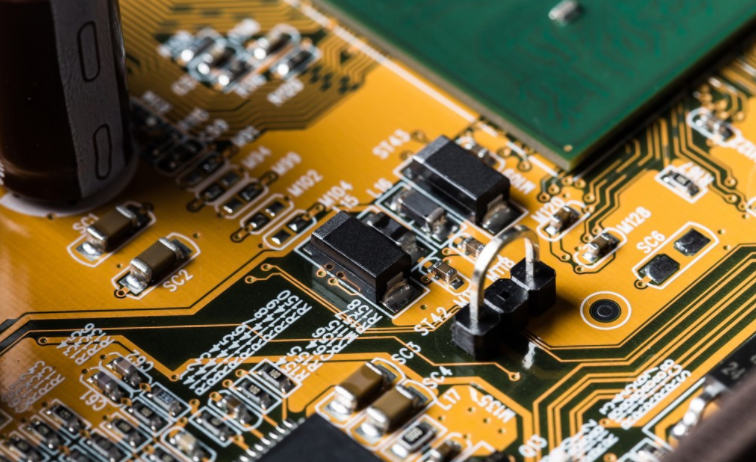
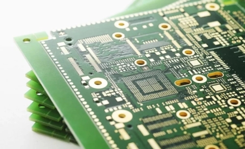
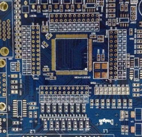
pcb board

2. Physical method of PCB recycling
Physical methods are based on the density, conductivity, magnetism, surface wettability and other physical properties of the data. The main process is disassembly and fracture. Separation and recovery of precious metals to deal with hazardous substances.
2.1. The general order of selective folding of electronic waste is: select reusable parts. Dismantle harmful parts and classify the parts of various materials. The disassembly method includes manual disassembly, mechanical disassembly and automatic disassembly. In order to realize the automatic disassembly of PCB, use the sink or hot air heating to dissolve the solder, and then use the vacuum fixture or robot to remove the components on the PCB surface.
2.2 Fracture PCB is broken by impact crushing and shearing. At present, the successful application is the ultra-low temperature freeze crushing technology, which can crush the toughness data after low-temperature embrittlement to 0.074mm, thus completely separating metals and nonmetals. Two stage crushing technology is often used in China, that is, the shear crusher is used to roughly crush PCB particles, and then the dry or wet crusher is used to finely crush PCB particles to the specified particle size to achieve complete separation of metal and non-metal.
2.3 Crushing data are sorted according to the density, fineness and magnetic conductivity of each component, usually including dry and wet sorting. Dry separation includes dry screening, magnetic separation and electrostatic separation. Density and eddy current separation, etc. Wet separation includes hydrocyclone classification flotation hydraulic vibrating screen, etc. The recovery rate of wet separation is high, but the cost is also high. The reagents used pollute the environment. The separated waste residue and waste liquid cause secondary pollution to the environment. The cost of dry separation is relatively low, and the main disadvantage is the low separation rate of fine particles.
Density ordering: The movement of particles in the fluid depends not only on the particle density, but also on their size and shape. In order to reduce the scale effect and control the relative motion of particle density. The metal in PCB was separated and enriched, and the effect of air separation and enrichment of metal in different particle sizes was studied.
The physical recovery of PCB board has the advantages of simple process, easy to scale, relatively small secondary pollution, low energy consumption, low cost, high separation efficiency, and meets the requirements of environmental protection and recycling. However, due to the overlap of various physical properties, complete separation between metals cannot be achieved, and the initial investment is large.
The above is the explanation given by the editor of pcb circuit board company.
If you want to know more about PCBA, you can go to our company's home page to learn about it.
In addition, our company also sells various circuit boards,
High Frequency Circuit Board and SMT chip are waiting for your presence again.


