PCB design of intelligent wearable device: intelligent bracelet
As a popular product form in recent years, intelligent wearable devices, especially smart bracelets, have attracted more and more attention. Although not everyone can use it, the emergence of smart bracelets has indeed brought new challenges to PCB design and processing.
An intelligent bracelet is usually composed of RF circuit unit, clock circuit unit, memory circuit unit, sensor circuit unit, and master MCU unit. The circuit PCB usually needs to be assembled in a small volume for single-sided or double-sided mounting. The circuit board is mainly composed of four or six layers.
Since so many functions are concentrated on a small PCB, PCB designers should pay special attention to the layout and wiring of the bracelet. Now Mr. Chen has summarized some precautions for everyone.
First, the layout shall be reasonably divided and the wiring protection shall be paid attention to.
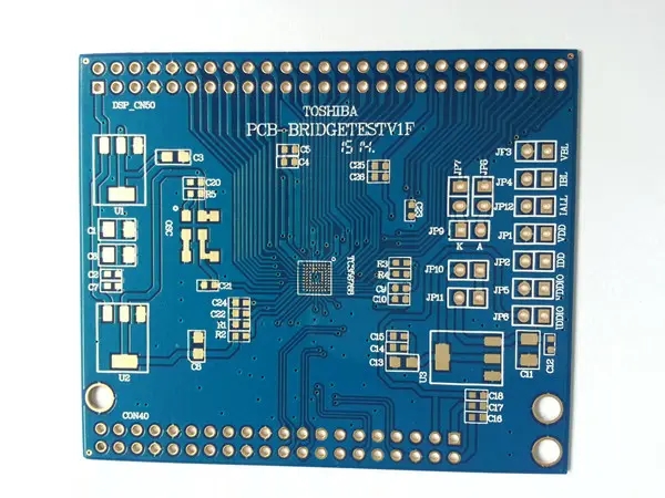
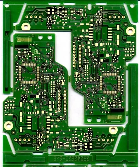
From the PCB circuit board above, it can be seen that each part of the circuit of the smart bracelet (marked with boxes of different colors) has a good partition: since the smart bracelet is a collection of digital circuit components, as long as the matching resistance and capacitance are well distributed in the circuit design, the circuit modules with certain functions can be completed, which makes the circuit design more concise and easy to find. Although some sensor circuit units use analog circuit technology for data acquisition, once the module is designed as a module, data communication and information transmission can be completed through the corresponding connection interface.

In the layout of circuit modules, on the one hand, attention should be paid to the clock circuit and crystal oscillator circuit to reach the target through the shortest path; on the other hand, attention should be paid to avoiding data lines when routing the clock to prevent interference from affecting the stability of the system.
During wiring, it is necessary to protect the key wiring, such as whether the clock generation circuit and crystal oscillator circuit are protected by copper coating and whether the ring ground protection is carried out. Generally, protection will be carried out in the design. For the crystal oscillator part, copper digging is required.
Second, handle the RF circuit well.
The smart bracelet needs to be linked with the mobile phone when it is used. Therefore, the radio frequency part is the key part. In this part of the design, special attention must be paid. Now the smart bracelets on the market are all wireless data transmission based on Bluetooth, so the emphasis is on the processing of Bluetooth RF. If the smart bracelet is only used for data transmission and does not need to transmit sound and music, then low-power Bluetooth is the best choice. In the design, the shape of the Bluetooth antenna, the antenna layout, and the shell material of the smart bracelet are all important factors that affect the performance of the smart bracelet. In the design process of smart bracelet PCB, an excellent RF antenna engineer is particularly important.
Third, ESD protection shall be well done.
Circuit ESD is a very important and non negligible part of PCB design. Today, we emphasize the importance of ESD to smart bracelet products. Different countries and regions have different standards for different products or the same product ESD requirements. In order to make the product pass relevant tests, ESD protection design shall be carried out during design, and ESD testing shall be carried out after the design is completed to ensure that the product can adapt to electronic testing in the local market.
Finally, the system upgrade interface is reserved.
The function upgrade of a smart bracelet is of great significance to users or enthusiasts. If the software of a product is upgraded at an appropriate time (it may be that the hardware is designed to some functions in the early stage and the software fails to catch up with the market, or it may be that some software bugs have been repaired), this indicates that the product is still in the process of continuous research and development, which is a good psychological compensation for users. Now, there are usually two ways to upgrade the software of the smart bracelet: through USB interface and wireless push. As for which method to adopt, it needs to be determined in the early planning and software and hardware planning.
PCB manufacturers, PCB designers and PCBA manufacturers will explain the PCB design of intelligent wearable devices: smart bracelets


