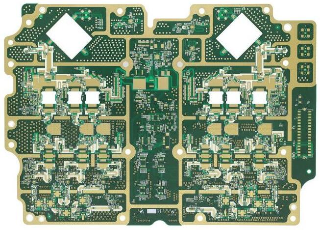
What is HDI PCB
High density interconnect (HDI) PCB represents one of the fastest growing technologies in PCBA processing. Because its circuit density is higher than that of traditional PCBA circuit boards, HDI PCB designs can include smaller through-hole and capture pads, as well as higher connection pad density. HDI plates contain blind and buried holes, and typically contain pores with a diameter of 0.006 or less.

By using HDI technology, designers can now place more components on both sides of the original PCB as needed. Now with the development of through-hole and blind hole technology in pads, it allows designers to place smaller components closer together. This means faster signal transmission and significantly reduced signal loss and cross delay.
HDI PCB often appears in mobile phones, touch screen devices, laptops, digital cameras, 4G network communications, and also plays an important role in medical equipment.
Advantages of HDI PCB
The most common reason for using HDI technology in PCBA production is to significantly increase package density. The space obtained by the more refined track structure can be used for components. In addition, the reduction of overall space requirements will result in smaller board sizes and fewer layers.
In SMT processing, usually FPGA or BGA can provide 1mm or less spacing. HDI technology makes wiring and connection easy, especially when wiring between pins.
HDI PCB improved functions:
1. Denser trace routing
2. More stable power supply
3. Reduce interference inductance and capacitance effect
4. Improve signal integrity in high-speed design
Use HDI PCB to accelerate development
1. Easier placement of SMD components
2. Faster routing
3. Reduce frequent repositioning of components
4. More element space (via Via in Pad)


