Application of Copper and Nickel Plating on PCB
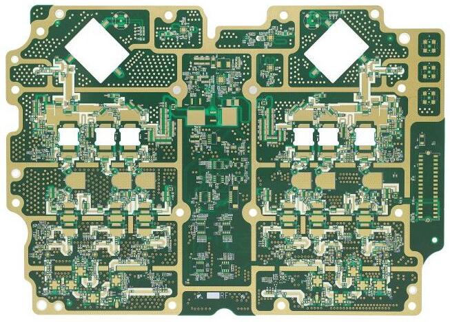
Electroplating is an important process in the production of metal products PCB Coated PCB s vary with the use of circuit boards This paper briefly introduces the efficiency and application of copper and nickel coatings produced by Circuit board manufacturer kingford
1. Effectiveness and use of copper plating layer on PCB
The copper coating of PCB is rose colored, soft, flexible, easy to polish, and has good thermal conductivity and conductivity. However, it is easy to oxidize in the air and quickly lose its luster, so it is not suitable as the "surface" layer of protective decorative coatings.
The copper coating on PCB is mainly used as the "bottom layer" of steel multi-layer coating. It is also often used as the "bottom layer" of tin, gold and silver plating. Its function is to improve the adhesion between the base metal and the surface or (or intermediate) coating, and promote the deposition of the surface coating. When the copper coating of PCB board has no holes, the corrosion resistance of the surface coating can be improved. For example, here we can explain the advantages of using thick copper and thin nickel electroplating processes in protective decoration multi-layer electroplating, and can save precious metal nickel.
pcb board

2. Effectiveness and application of nickel coating on PCB
Nickel metal has a strong passivation ability. It can quickly generate a very thin passivation film on the surface of parts, which can resist atmospheric and some acid corrosion. In addition, the nickel coating of this PCB has a high stability in the air. In a simple nickel salt electrolyte, a very fine crystalline coating can be obtained, which has excellent polishing efficiency. The nickel coating on polished PCB board has mirror luster, while maintaining its luster in the atmosphere for a long time. In addition, the nickel coating of PCB board has high hardness and wear resistance. According to the efficiency of nickel coating on PCB, it is mainly used as the bottom layer, intermediate layer and surface layer of protective decoration coating, such as nickel chromium coating, nickel copper nickel chromium coating, copper nickel chromium coating and copper PCB nickel coating.
Due to the high porosity of nickel coating on PCB, only when the coating thickness is more than m and is 25m, there is no hole. In general, this nickel coating is not used as a protective coating.
The output of nickel plating on PCB is very large, and the consumption of nickel plating accounts for about 10% of the total global nickel output.
3. PCB circuit board copper plating process
Electroless copper plating, also known as copper precipitation or porous (PTH), is an autocatalytic redox reaction. First, the active particles on the surface of the insulating base are treated with an activator. Palladium particles are usually used (Palladium is a very expensive metal, which is expensive and has been increasing. In order to reduce costs, a practical colloidal copper process is currently running abroad). Copper ions are first reduced on these active metal palladium particles. These reduced copper nuclei themselves become the catalytic layer of copper ions, enabling the reduction of copper to continue on the surface of these new copper nuclei. Electroless copper plating has been widely used in our PCB manufacturing industry. At present, electroless copper plating is the most widely used method for PCB hole metallization. The metallization process of PCB holes is as follows:
Drilling+deburring of sanded plate+cleaning of top plate+ten pairs of cleaning+chemical roughening of micro etching+double cleaning One pre leaching treatment One colloid palladium activation treatment One pair of cleaning+gel removal treatment (accelerated)+double cleaning+copper leaching One pair of cleaning Ten top plates+copper leaching 11 times Copper leaching 10 times Cleaning one time+drying.


