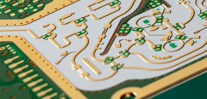
Modeling and analysis of electromagnetic compatibility of switching power supply PCB
In the modeling and analysis of the electromagnetic compatibility of PCB in switching power supply, the interference path of switching converter noise provides coupling conditions for the interference source and the interfered equipment, and the study of its common mode interference and differential mode interference is particularly important The high frequency models of the main circuit components and the circuit models of common mode and differential mode noise are mainly analyzed, which provides a useful help for the electromagnetic compatibility optimization design of switching power supply PCB Common mode interference and differential mode interference of switching power supply have different effects on the circuit Generally, differential mode noise dominates at low frequencies, and common mode noise dominates at high frequencies. The radiation effect of common mode current is usually higher than that of differential mode current The radiation effect is much larger. It is necessary to distinguish the differential mode interference from the common mode interference in the power supply In order to distinguish differential mode interference from common mode interference, we first need to study the basic coupling mode of switching power supply. On this basis, we can establish the circuit path of differential mode noise current and common mode noise current The conductive coupling of switching power supply mainly includes: circuit conductive coupling, capacitive coupling, inductive coupling and the mixture of these coupling methods
PCB board

1. Common-mode and differential-mode noise path models
In the switching power supply, the coupling capacitance CW between the primary and secondary windings of the high-frequency transformer, the stray capacitance CK between the power tube and the radiator, the parasitic parameters of the power tube itself, and the mutual coupling between printed wires are formed Mutual inductance, self inductance, mutual capacitance, self capacitance, impedance and other parasitic parameters form common mode noise and differential mode noise paths, thus forming common mode and differential mode conducted interference Based on the analysis of the resistance parasitic parameter model, the noise current path model of the converter can be obtained from the inductance and capacitance of power switching devices, transformers and printed wires
2. High-frequency model of the main components of the circuit
The internal parallel induction and capacitance of the power switch tube affect the high frequency performance of the circuit These capacitors allow high-frequency interference leakage current to flow to the metal substrate. There is a stray capacitor CK between the power tube and the radiator For safety reasons, the radiator is usually grounded to provide a common mode noise path When PWM converter works, common mode noise will be generated with the operation of switching equipment For half bridge converter, the drain voltage of switch Q1 is always U1, and the source potential changes between 0 and U1/2 with the change of switch state; The source potential of Q2 is always 0, and the leakage potential is 0 and U1/2. In order to keep a good contact between the switch tube and the radiator, insulating gaskets or insulating silica gel with good thermal conductivity are usually added between the bottom of the switch tube and the radiator This is equivalent to a parallel coupling capacitor CK between point a and ground When the state of switches Q1 and Q2 changes, the potential of point A changes, and the noise current Ick will be generated on CK, as shown in Figure 2 The current flows from the radiator to the main housing and chassis, that is, the ground has a coupling impedance with the main power line, forming a common mode noise path as shown in the dotted line in Figure 2 Therefore, common mode noise current generates voltage drop on the coupling impedance Z between the ground and the main power line, forming common mode noise Isolation transformer is a widely used power line interference suppression measure Its basic function is to realize power isolation between circuits and solve mutual interference between equipment caused by grounding circuit For an ideal transformer, it can only carry differential mode current and cannot carry common mode current. This is because for common mode current, the potential between the two terminals of the ideal transformer is the same, so it cannot generate magnetic field on the winding, or there may be no common mode current path, which plays a role in suppressing common mode noise The actual isolation transformer has a coupling capacitor CW between the primary side and the secondary side The coupling capacitor is generated by the non dielectric and physical gap between transformer windings, which provides a path for common mode current
Common isolation transformer can restrain common mode noise to some extent, but due to the distributed capacitance between windings, the effect of restraining common mode interference decreases with the increase of frequency The common mode interference suppression of ordinary isolation transformers can be estimated by the ratio of the distributed capacitance between the first and second stages to the distributed capacitance of the equipment to the ground Generally, the distributed capacitance between the primary and secondary is several hundred pF, and the distributed capacitance to ground is several to tens of nanovolts. In addition, the attenuation value of this common mode interference is about 10 to 20 times, that is, 20 to 30 dB In order to improve the ability of isolating transformer to suppress common mode noise, the key is to have a small coupling capacitor Therefore, you can add a mask layer between the primary and secondary of the transformer The shield has no adverse effect on the energy transmission of the transformer, but it will affect the coupling capacitance between windings In addition to suppressing common mode interference, the isolation transformer with a mask layer can also suppress differential mode interference by using a mask layer The specific method is to connect the shielding layer of the transformer to the neutral end of the primary winding For 50Hz power frequency signal, due to the high capacitive reactance formed by the primary and mask layers, it can still be transmitted to the secondary side through the transformer effect without attenuation For differential mode interference of higher frequency, as the capacitance reactance between the primary and the mask layer becomes smaller, this part of interference returns to the power grid directly through the distributed capacitance and the connection between the mask layer and the primary neutral terminal, instead of entering the secondary circuit Therefore, it is very important to model the high frequency of the transformer, especially many parasitic parameters of the transformer, such as leakage inductance, distributed capacitance between the primary and secondary sides, etc, It has a significant impact on the level of common mode electromagnetic interference and must be considered In practice, impedance measuring equipment can be used to measure the main parameters of transformer, so as to obtain these parameters and conduct simulation analysis The DC electrolytic capacitor Cin in the half bridge circuit has corresponding series equivalent inductance ESL and series equivalent resistance These two parameters will also affect the high frequency efficiency of the circuit Generally, ESL is about tens of nH In practical analysis, the high-frequency equivalent parasitic parameters of passive components such as resistors, inductors and capacitors can be measured by high-frequency impedance analyzer, and the high-frequency models of power devices can be obtained from the model library of circuit simulation software Another factor that has a greater impact on the high-frequency noise of a circuit is the mutual coupling of the printed conductors (striplines) on the printed board. When high amplitude transient current or rapidly rising voltage occurs near the conductor, there will be interference problems The coupling of printed wires is usually characterized by the capacitance and mutual inductance of circuits and wires Capacitive coupling leads to coupling current, and inductive coupling leads to coupling voltage PCB layer parameters, signal line track and its spacing will affect these parameters The main difficulty in establishing the high frequency model of PCB trajectory and selecting the parasitic parameters between tracks is to determine the tissue length capacitance and tissue length inductance of PCB trajectory There are generally three methods that can be used to determine the inductance and capacitance matrix components: (1) Finite Difference Method (FDM); (2) Finite Element Method (FEM); (3) Momentum Method (MOM). After determining the organization length matrix, a high frequency simulation model of the printed circuit board traces can be observed through multi conductor transmission line or partial element equivalent circuit (PEEC) theory Cadence software is a powerful EDA software Its SpectraQuest tool can perform signal integrity and electromagnetic compatibility analysis on the following objects: PCB boards s It can also be used for high-frequency modeling of PCB trajectories to achieve a given structure The parameters are from PCB board, parasitic parameter matrix of inductance, capacity, and the resistance that generates any shape of printed wire trace, and then use PEEC theory to conduct electromagnetic compatibility simulation analysis
The above is the explanation given by the editor of pcb circuit board company.
If you want to know more about PCBA, you can go to our company's home page to learn about it.
In addition, our company also sells various circuit boards,
High frequency circuit board and SMT chip are waiting for your presence again.


