Process flow of SMT chip processing and equipment required for SMT chip
The rapid development of industry is both an opportunity and a challenge for the electronic industry. Today's electronic products are characterized by miniaturization, thinness and versatility, which puts forward more stringent requirements for circuit boards. In order to achieve these miniaturized and highly integrated circuits, SMT chip processing technology is required.

The following is a detailed understanding of the SMT chip processing process:
1. Programmed placement machine:
Program the coordinates of the placement components according to the sample BOM placement location map provided by the customer. Then, check the first piece with the SMT chip processing data provided by the customer.
2. Printing solder paste:
The solder paste is stenciled onto the bonding pad of the electronic component SMD on the PCB board to prepare for the welding of the components. The equipment used is a screen printing machine (printing machine), which is located at the front end of the SMT chip processing production line. Wanlong Jingyi adopts GKG GT full-automatic printing machine and international brand KOKi solder paste, which can not only accelerate production efficiency, but also ensure welding quality.
3. Patch:
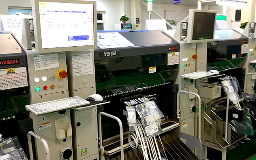
It is to accurately install the electronic components SMD on the fixed position of PCB. The equipment used is the mounting machine, which is located behind the screen printing machine in the SMT production line. The SMT machine used by Wanlong Jingyi is from Yamaha YS12 high-speed SMT machine. This equipment has its own air compressor, which does not need an external air compressor. It can stack up 10 0201 materials without toppling. The mounting precision is very high. It is one of the most accurate mounting equipment in all SMT systems at present.
4. Reflow soldering:
It is mainly used to melt the solder paste at high temperature and firmly weld the electronic components SMD and PCB board after cooling. The equipment used is the reflow soldering furnace, which is located behind the SMT mounter in the SMT production line. The PCB factory should adopt the new 9-temperature zone reflow welding machine in the United States, with three cooling zones and water tower cooling. Different from the U-shaped reflow soldering heat pipe of other companies, the reflow soldering in the PCB factory uses the sandwich structure of upper and lower heating plates, which can make the heating more balanced.
5. Cleaning:
Its function is to remove harmful welding residues such as flux on the assembled PCB board. The equipment used is a cleaning machine, which can be either online or offline, and its location can be flexible.
6. Test/Inspection:
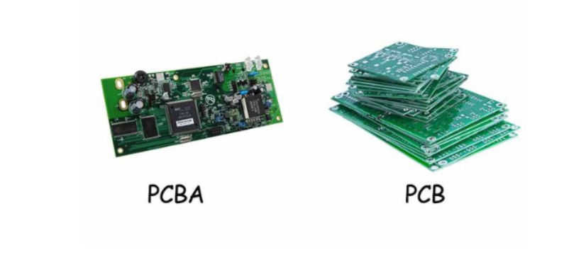
The welding quality inspection of PCBA board after reflow welding generally includes the following aspects: surface patch or through-hole plug-in, single or double side, number of components (including sealing feet), solder joints, electrical and appearance characteristics, focusing on the test and inspection of the number of components and solder joints. Wanlong Jingyi adopts offline AOI detector, X-RAY detector, LCR bridge detector, 60x digital electron microscope and other high-precision testing equipment to ensure that the quality of each product reaches the standard.
7. Packaging:
The qualified products shall be separated for packaging. The commonly used packaging materials are anti-static bubble bags, electrostatic cotton, and blister discs. There are two main packaging methods. One is to separate the packaging with anti-static bubble bags or static cotton in rolls, which is currently the most commonly used packaging method; The second is to customize the blister disk according to the size of PCBA. PCBA boards that are sensitive to needles and have vulnerable patch elements are placed in blister trays and unpacked.
This article mainly introduces the process flow of SMT chip processing and the equipment required for SMT chip


