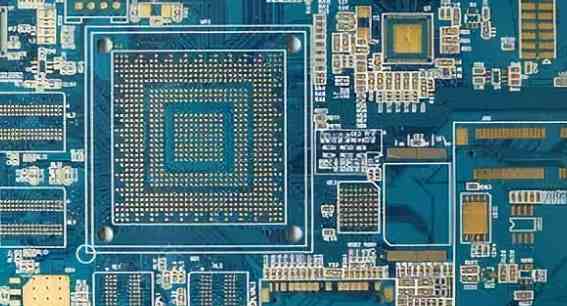
land, the basic unit of surface mount assembly, used to form the land pattern of the circuit board, that is, various combinations of pads designed for special component types. There is nothing more frustrating than poorly designed pad construction. When a pad structure is not designed correctly, it is difficult and sometimes impossible to reach the desired weld points. The English words for Pad are Land and Pad, which are often used interchangeably. Functionally, however, Land is a two-dimensional surface feature for surface-mountable components, while Pad is a three-dimensional feature for plugable components.
As a general rule, Land does not include PTH (plated through-hole). A by-pass hole (via) is an electroplated through-hole (PTH) that connects different circuit layers. The blind via connects the outermost layer to one or more inner layers, while the buried bypass hole connects only the inner layer.
As noted earlier, pad Land usually does not include plating through holes (PTH). The PTH in a pad Land will carry away a considerable amount of solder during the welding process, in many cases producing solder deficient solder joints. In some cases, however, PCB design component wiring density forces a change to this rule, most notably for CSP, chip scale packages. Below 1.0mm(0.0394") spacing, it is difficult to route a wire through the "maze" of pads. A blind by-pass hole and a microvia hole are created in the pad to allow direct wiring to another layer. Because these bypass holes are small and blind, they do not suck up much solder, resulting in little or no effect on the amount of tin in the solder joint.
There is a lot of industry literature out of IPC(Association Connecting Electronics Industries), EIA(Electronic Industry Alliance) and JEDEC(Solid State Technology Association) should be used when designing pad structure. The main document is IPC-SM-782 Standard for Surface Mount Design and Pad Construction, which provides information on pad construction for surface mount components. When J-STD-001 Requirements for Welding Electrical and electronic assembly and IPC-A-610 Acceptability of Electronic Assembly are used as welding point process standards, pad construction shall conform to the intent of IPC-SM-782. If the pad deviates significantly from the IPC-SM-782, it will be difficult to reach the weld points that comply with J-STD-001 and IPC-A-610.
Component knowledge (i.e. component structure and mechanical size) is the basic necessary condition for the design of pad structure. IPC-SM-782 makes extensive use of two component literature: EIA-PDP-100, Registration and Standard Mechanical Form of Electronic Parts, and JEDEC 95, Registration and Standard Form of Solids and Related Products. Arguably the most important of these documents is the JEDEC 95 publication, as it deals with the most complex components. It provides mechanical drawings of all registrations and standard shapes of solid components.
Abbreviations of components are defined based on package characteristics, materials, terminal positions, package types, pin forms, and number of terminals. Feature, material, location, form, and quantity identifiers are optional.
Encapsulation feature: A single or multiple letter prefix that identifies features such as pitch and contour.
Packaging material: A single-letter prefix that identifies the main packaging material.
Terminal position: A single-letter prefix that identifies the terminal position relative to the package outline.
Package Type: A two-letter mark indicating the type of shape of the package.
Pin New: A single - letter suffix to confirm pin form.
Number of terminals: A one -, two -, or three - digit suffix indicating the number of terminals.
Surface Mount A simple list of packaging feature identifiers includes:
E expanded spacing (> 1.27 mm).
F close spacing (< 0.5mm); Limited to QFP components.
S contraction spacing (< 0.65mm); All components except QFP.
T-thin (1.0mm body thickness).
A simple list of surface mount terminal position identifiers includes:
Dual pins are on opposite sides of a square or rectangular package.
Quad pins are on the four sides of a square or rectangular package.
Surface Mount A simple list of package type identifiers includes:
CC chip carrier package structure.
FP flat pack package structure.
GA grid array package structure.
SO small outline package structure.
A simple list of pin form identifiers for surface mount includes:
B A straight handle or spherical pin structure; This is a non-compliant pin form
F A flat pin structure; This is a non-compliant pin form
G A fin pin structure; This is a compliant pin form
J A "J" shaped curved pin structure; This is a compliant pin form
N a pinless structure; This is a non-compliant pin form
S An "S" shaped pin structure; This is a compliant pin form
For example, the acronym F-pqFp-G208, describes 0.5 mm(F) plastic (P) square (Q) flat package (FP), fin pin (G), terminal number 208.
Detailed tolerance analysis of elements and plate surface features (i.e. pad structure, reference points, etc.) is necessary. PCB board IPC-SM-782 explains how to perform this analysis. Many components (especially closely spaced components) are designed in strict metric units. Do not design English pad construction for metric components. Cumulative structural errors result in misfits and are completely unusable for closely spaced components. Remember, 0.65mm is 0.0256" and 0.5mm is 0.0197".


