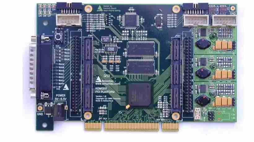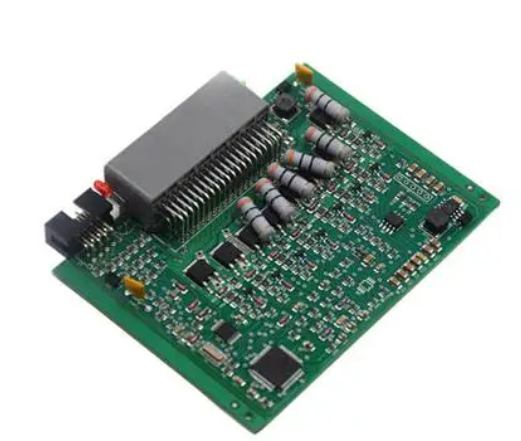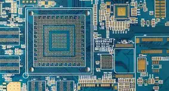
PCBA circuit board three anti-paint is mainly used to protect PCBA board from environmental erosion, the use of three anti-paint PCBA circuit board has moistureproof, aging resistance, ozone corrosion resistance and other properties, kingford to introduce the use of PCBA circuit board three anti-paint matters for attention:
First, the precautions of coating three anti-paint
1, can not let the PCB board surface leakage, paint flow, semi-humid phenomenon
2. In order to protect the pasted components and pad, the three anti-paint should be ensured to be uniform, bright and smooth
3, can not let the surface of the paint layer pinholes, bubbles and other phenomena
4, do not need to protect the devices or components do not need to brush with three anti-paint
5, should ensure that the printed board after the three anti-paint clean, no damage to components
6. There are no dirt, handprints, ripples, shrinkage holes, dust and other defects and foreign objects on the board surface and components, no powder, no peeling phenomenon
2. List of components that cannot be coated with three anti-paint
1, high power with cooling surface or radiator components, power resistance, power diode, cement resistance
2, dip switch, adjustable resistance, buzzer, battery holder, safety seat (tube), IC seat, touch switch
3. All types of sockets, pins, wiring terminals and DB heads
4, plug or stick type LED, digital tube
5. Other parts and devices that cannot use insulating paint according to the drawings
6, PCBA board card screw hole can not brush coated with three anti-paint
Moisture is always the main factor affecting PCBA circuit board, and the three anti paint can protect PCBA board from moisture.
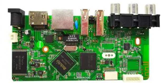
2. Problems needing attention in PCB wave soldering process
Wave soldering is a batch welding process for manufacturing PCB circuit boards, mainly used for through hole components welding. The following to introduce the PCB circuit board wave soldering process need to pay attention to what problems
1. There is green oil in the element hole, leading to poor tin plating in the hole. The green oil in the hole should be kept below 10 percent of the hole wall and the number of holes in the internal green oil should be below 5 percent.
2, leading to poor tin plating in the hole may be too small coating thickness.
3. The coating thickness on the component hole wall is not enough, resulting in poor tin plating in the hole. Generally, the thickness of the pore wall should be above 18 microns.
4. The hole wall is too rough, resulting in poor tinning or pseudo-welding in the hole.
5, the hole is wet, resulting in pseudo welding or bubbles. Packaging the PCB when it is not dry or cooled, and leaving it for a long time after unpacking, etc., will result in moisture in the hole.
6. The main factor leading to welding failure may be that the hole size is too small, the parts can not be inserted into the hole, or the positioning hole is offset, the parts can not be inserted into the hole.
The above is the introduction of "Problems needing attention in PCB wave soldering process". I hope it will be helpful to you. For more PCBA information, please pay attention to kingford's content update!


