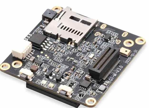
Guidelines for PCB design and layout of wiring
It is critical for board designers to lay out their boards to create the best possible signal and power integrity. Components shall be placed in a good position for short and direct wiring. At the same time, the boards must be laid out so that all the networks can be fully wired. Trying to balance these requirements can be quite a challenge in high-density design. The first PCB design layout guide sets design rules and constraints for wiring.
Design rules and constraints
Technically, configuration design rules and constraints should be included in the parameters and Settings. However, since most of the rules apply directly to tracing routes, we have included this guide here. Rules and constraints are used to control cable width and spacing and can be set for a single network, a network group called a network class, or as the default for all non-specified networks. Design rules are also used to control which holes are selected for different networks, route lengths, and match lengths, and which board layers are allowed for routing specific networks and routing topologies. In addition, design rules are used to control component spacing, silkscreen rules, mechanical clearance, and many other constraints.
Signal and power integrity
In order to achieve better performance and signal integrity, PCB layout designers need to follow the specific requirements of different circuit routing. Design rules and constraints help here -- allowing the designer to enter physical wiring parameters into the CAD system for wiring. Although the exact value can vary depending on the needs of the board, designers often set rules to ensure that the following guidelines are followed:
Short and direct high-speed transmission line routing.
Line width, spacing, and allowable layers for controlled impedance wiring.
Match the specified line length and length tolerance of the length wiring.
Difference requirements for cable width and spacing.
Width and spacing of sensitive signals such as clocks and control lines.
Orifice types of different networks.
Line width and spacing of analog circuits.
High current power supply circuit line width and copper weight.
Another important guideline to keep in mind is to avoid areas where digital circuits cross analog wiring and vice versa when wiring in a mixed-signal design.
Guide to effective power supply and ground plane
For modern high-speed designs, the preferred grounding strategy is usually to use one or more continuous connecting strata on the inner layer. This provides better EMI protection and ensures a clear signal path, which improves overall signal integrity. Avoid wiring in any ground gaps in areas where the ground plane is disconnected due to a unique circuit board profile or feature. Without contiguous and adjacent ground planes for the signal to use as a clear return path, your design can produce a lot of undesirable noise. Here are some power and ground floor guidelines to keep in mind:
The grounding layer needs to be adjacent to the signal layer in the board stack with high speed wiring. This will help shield the high-speed wiring from interference and provide a good reference plane for the signal return path.
Use heat dissipation pads and carefully manage the power supply and ground connections to the plane. Cushioning spokes must be wide enough to withstand high currents while eliminating the opportunity for these connections to act as radiators.
Carefully plan the power connections and split the power plane to ensure adequate delivery of power to all connected components throughout the board.
Avoid wiring analog and digital circuits simultaneously in mixed-signal designs
Silk screen and PCB test guide
With the board design complete, it's time to turn your attention to completing the layout by cleaning up the silk-screen layer and adding test points. Reference marks, part numbers, and other company information are inked on the circuit board by a silkscreen process. Designers often use "screen printing" layers in their CAD systems to design these marks.

To ensure that the silk screen marks are readable, designers follow the following guidelines:
Line width should not be less than 6 mil.
Font size should not be less than 50 mil.
Renames component reference indicators according to the corporate grid pattern to help locate specific parts on the board.
Move and rotate reference markers to make them easy to read.
Include polarity and a pin mark where needed.
The test point is critical to the mass production of circuit boards for automatic assembly verification. Each network in the design should have a test point, whether that test point is an existing through-hole pin, through-hole, or an added surface mount test spot pad. The test point should be at least 50 mils clear from other board objects, such as components or pads, and at least 100 mils away from the edge of the board. However, these values may vary from vendor to vendor, so be sure to check what the manufacturer's test point requirements are first.


