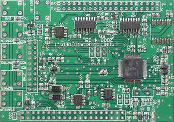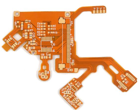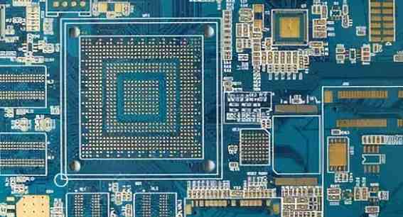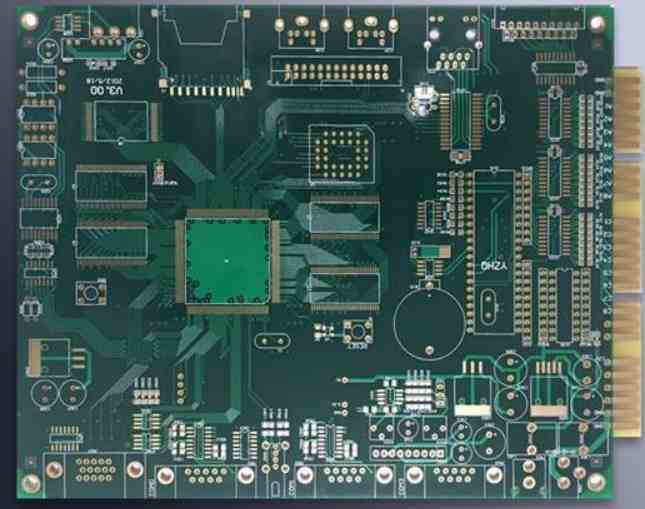
The technical realization process of PCB copying board is simply to scan the circuit board of the copying board, record the location of the components in detail, and then disassemble the components to make BOM and arrange material procurement. The empty board is scanned into pictures, processed by the copying software and restored to the PCB board drawing file, and then the PCB file is sent to the plate maker to make the board. After the board is made, the purchased components are welded to the PCB board, and then the circuit board is tested and debugged.
Double panel copying method
1. Scan the upper and lower layers of the circuit board and save two BMP pictures.
2. Open the board copy software Quickpcb2005 and click "File" "Open base" to open a scanned image. Use PAGEUP to enlarge the screen, see the pad, place a pad according to PP, see the line line according to PT...... Just like a child's sketch, draw it in this software and click "Save" to generate a B2P file.
3. Click "File" and "Open base Map" to open another layer of scanning color map;
4. Click "File" "Open" again to open the previously saved B2P file. We can see the board we just copied, stacked on this picture -- the same PCB board, the holes are in the same position, but the line connection is different. So we press "Options" - "Layer Settings", here to turn off the display of the top layer of lines and silk screen, leaving only smultiple layer of holes.
5. The holes on the top layer are in the same position as the holes on the bottom picture. Now we can trace the bottom line as we did in childhood. Click "Save" again - the B2P file now has the top and bottom layers of data.
6. Click "File" "Export to PCB file", you can get a PCB file with two layers of data, which can be changed to the board or the schematic diagram or directly sent to the PCB platemaking factory for production.
7. How to select a cleaning agent for the PCB circuit board
In PCB printed circuit board components, there are three main ways of binding or adhesion between pollutants and components, which are molecule-to-molecule binding, also known as physical bond binding; Bonding between atoms, also known as bonding; Contaminants are embedded in particles in materials such as welded masks or electroplated deposits, known as "inclusions".
The core of the cleaning mechanism is to destroy the chemical bond or physical bond between pollutants and PCB printed circuit boards, so as to achieve the purpose of separating pollutants from the components. Since this process is endothermic, it must be supplied for this purpose.
Using appropriate solvent, through the dissolution reaction and saponification reaction between pollutants and solvents to provide energy, can destroy the binding force between them, so that pollutants dissolve in the solvent, so as to achieve the purpose of removing pollutants.
In addition, specific water can be used to remove contaminants left by the water-soluble flux to the components.
Because PCB printed circuit board components are polluted to different degrees after welding, different types of pollutants and different products have different requirements for the cleanliness of components after cleaning, therefore, there are many kinds of cleaning agents available. So, how to choose the right cleaning agent? The following SMT processing plant technicians to introduce some basic requirements for cleaning agents.
(1) wettability. For a solvent to dissolve and remove contaminants from SMA, it must first be able to moisten the contaminated PCB, expand and moisten onto the contaminant.
The wetting Angle is the main factor that determines the degree of wetting. The best cleaning condition is that the PCB expands spontaneously, and the wetting Angle is close to 0°.
(2) Capillary effect. A solvent with good wetting capacity does not necessarily guarantee effective removal of contaminants. The solvent must also be easy to cure, enter and exit these narrow Spaces, and be able to recycle until the contaminant is removed. The solvent is required to have a strong capillary effect in order to penetrate these dense gaps. Commonly used cleaning agent capillary permeability, it can be known that the capillary permeability of water is the largest, but its surface tension is large, so it is difficult to discharge from the gap, resulting in low exchange rate of cleaning water, difficult to effectively clean. Although the capillary permeability of chlorinated hydrocarbon mixtures is low, the surface tension is also low. Therefore, considering the two properties, this kind of solvent has a better cleaning effect on the component pollutants.
(3) viscosity. The viscosity of solvent is also an important property that affects the effective cleaning of solvent. In general, other things being equal, the higher viscosity of the solvent, the lower exchange rate in the slit on the SMA, which means that more force is needed to get the agent out of the slit. Therefore, the low degree of solvent helps it to complete multiple exchanges in the slit of SMD.
(4) Density. A high density solvent should be used to clean the components if other requirements are met. This is because, during the cleaning process, when the solvent vapor condenses on the components, gravity helps the condensed solution flow downward, improving the cleaning quality. In addition, the high density of the solution also helps to reduce its emission to the atmosphere, thus saving materials and reducing operating costs.
(5) boiling point temperature. Cleaning temperature also has a certain effect on cleaning efficiency. In most cases, the temperature of the solvent is controlled at or near the boiling point. Different solvent mixtures have different boiling points and the change of solvent temperature mainly affects its physical properties. Vapor condensation is an important part of the cleaning cycle. The increase in the boiling point of the solvent allows the acquisition of vapor at a higher temperature, and higher vapor temperatures lead to greater vapor condensation, which can remove a large amount of contaminants in a short time. This relationship is most important in on-line conveyor belt wave soldering and cleaning systems because the speed of the cleaning agent conveyor must be consistent with the speed of the wave welding conveyor.

(6) solubility. When cleaning SMA, the distance between components and substrate, between components, and between I/O terminals of components is very small. As a result, only a small amount of solvent can contact the pollutants under the components. Therefore, it is necessary to use solvents with high solubility, especially when cleaning is required to be completed within a limited time, as is considered in on-line conveyor belt cleaning systems. However, it should be noted that solvents with high solubility are also more corrosive to the parts being cleaned. Most of the solder paste and double wave welding using rosin based flux, so, in the comparison of the dissolution capacity of various solvents, the rosin based flux residue should be paid special attention to.
(7) Ozone destruction coefficient. With the continuous progress of society, people's environmental awareness is increasing, therefore, in the evaluation of the ability of cleaning agents at the same time, should also take into account the extent of damage to the ozone layer. For this reason, the concept of ozone destruction coefficient (ODP) was introduced, which is now based on the ozone destruction coefficient of CFC-113 (trichloroethane), that is, ODPCFC-113=1.
(8) Minimum value. The minimum value represents the maximum limit value that the human body can withstand when it comes into contact with the solvent, also known as the exposure limit. The operator is not allowed to exceed the minimum value of the solvent during daily work.
The above is the PCBA patch processing plant in the selection of cleaning agent, in addition to the above performance, should also take into account the economy, operation and equipment compatibility and other factors.


