Шэньчжэнь, район Баоань, улица Фуюн, улица Фуцяо, район 3, промышленный парк Лонгхуй 6
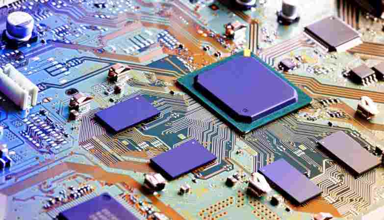
Connection between PCBA welding and steel wire mesh
This paper mainly describes the connection and difference between PCBA circuit board welding and steel wire mesh
The relationship between the die and SMT chip processing is inseparable. Many SMT chip processing practitioners must have a good grasp of the relationship between PCBA welding and mold. Today, this topic will explain to you about PCBA welding and mold.
The so-called mold is a thin steel plate. The size of the template is usually fixed to match the solder paste printer, but the thickness range of the template is 0.08mm, 0.10mm, 0.12mm, 0.15mm, 0.18mm, etc., for people to use as needed.
The purpose of the die is to allow solder paste to be printed on the circuit board during SMT chip processing. There will be many openings on the mold. When printing solder paste, smear the solder paste on the top of the mold, place the circuit board under the mold, and then brush the solder paste on the mold with a scraper (usually a scraper, because the solder paste is like a toothpaste like viscous substance) when squeezing the solder paste. It will flow down from the opening of the mold and stick to the top of the circuit board. After removing the template, you will find that the solder paste has been printed on the circuit board. To put it simply, the mold is like a cover, which needs to be prepared when painting. Solder paste is equivalent to paint. The cover is engraved with the graphic you want, and the required graphic will be displayed by painting on the cover.
According to the production process, SMT wire mesh can be divided into: laser template, electrolytic polishing template, electroforming template, step template, bonding template, nickel plating template, and etching template
Features: direct use of data files for production, reducing production errors;
The opening position of the SMT template is very accurate: the overall error is – 4mm;
The opening of the SMT template has a geometric pattern, which is conducive to the printing and molding of solder paste.
E.P. Stencil
After laser cutting, the electrolytic polishing template conducts post treatment on the steel plate by electrochemical method to improve the opening hole wall.
Features:
Smooth hole wall, especially suitable for ultra-fine spacing QFP/BGA/CSP;
Reduce the number of times to wipe the SMT template, and greatly improve the work efficiency.
E.F. Stencil
In order to meet the requirements of short, small, light and thin electronic products, ultra-fine volume (such as 0201) and ultra-fine asphalt (such as Ø BGA, CSP) are widely used. In this regard, SMT mold industry also put forward higher requirements, and electroforming model came into being.
Features: Different thicknesses can be made on the same model.
StepStencil
Due to the different requirements for solder paste amount when welding different components on the same PCB, the thickness of some areas of the same SMT template needs to be different, which leads to the voltage drop and voltage rise process templates.
Depressurization template: When welding specific components, partially dilute the template to reduce the amount of tin.
BondingStencil
The COB device has been fixed on the PCB, but it still needs a tin printed mounting process, which requires the use of a bonding template. The bonding template is to add a small cover at the PCB bonding position corresponding to the template to avoid the COB device from realizing the purpose of plane printing.
Nickel Plating Template (Ni. P. Stencil)
In order to reduce the friction between the solder paste and the hole wall, facilitate demoulding, and further improve the release effect of the solder paste, the nickel plated model combines the advantages of the laser model and the electroforming model.
Etching template
It is made of 301 steel plate imported from the United States. Etched steel mesh is suitable for PCB printing with corners and spacing greater than or equal to 0.4MM. It is suitable for copying and film use. According to different parts, CAD/CAM and exposure methods can be used at the same time. For zooming, it is not necessary to calculate the price based on the number of parts. Production time is fast. The price is cheaper than the laser model. Customers can easily archive films.
The classification of SMT steel mesh is basically divided into three categories according to production and processing methods, namely: chemical etching process, laser cutting process, electroforming process, etc.
Chemical etching
By applying corrosion protection agent on the metal foil, positioning the photosensitive tool with a pin, and then etching the metal foil from both sides simultaneously using a double-sided process, an opening is formed on the rigid grid, and the pattern is exposed on both sides of the metal foil.
Features: one-time molding, faster, lower price
Disadvantages: easy to form hourglass shape (insufficient etching); Or the opening size becomes larger (excessive etching); The objective factors (experience, medicine, film) have great influence, many production links, and large cumulative error, which are not suitable for the production of fine asphalt models; The production process is polluted, which is unfavorable to environmental protection.
Comparison between chemical etching (left) and laser cutting (right)
Laser cutting
The template product directly generated from the customer's original Gerber data has good location accuracy and reproducibility. Laser technology is the only process that allows rework of the current model.
Features: high data generation accuracy, less impact of objective factors; Trapezoidal opening is favorable for demoulding; It can be used for precision cutting; The price is moderate.
Disadvantages: cutting one by one, slow production speed.
Electroforming
It is an increasing rather than decreasing process by developing photoresist on the substrate (or core mold) to form an opening, and then plating the template atom by atom around the photoresist atom layer by layer.
Features: smooth hole wall, especially suitable for making superfine asphalt template
Disadvantages: the process is difficult to control, and the production process is polluted, which is unfavorable to environmental protection; The production cycle is long and the price is too high.
With the continuous development of printed circuit boards, the requirements for reliability are getting higher and higher, and 3D steel mesh will appear.
For step printed application circuit boards or substrates, the VectorGuard 3D mold made of electroformed nickel can not only print two heights at the same time, but also print different high and low surfaces, with a difference of up to 3mm Before this, if power transistors and other components need step printing support, they must be applied after the template is printed VectorGuard3D eliminates the dot coating step, optimizes the printing process, and effectively improves productivity
This paper mainly describes the connection and difference between PCBA circuit board welding and steel wire mesh
The relationship between the die and SMT chip processing is inseparable. Many SMT chip processing practitioners must have a good grasp of the relationship between PCBA welding and mold. Today, this topic will explain to you about PCBA welding and mold.
The so-called mold is a thin steel plate. The size of the template is usually fixed to match the solder paste printer, but the thickness range of the template is 0.08mm, 0.10mm, 0.12mm, 0.15mm, 0.18mm, etc., for people to use as needed.
The purpose of the die is to allow solder paste to be printed on the circuit board during SMT chip processing. There will be many openings on the mold. When printing solder paste, smear the solder paste on the top of the mold, place the circuit board under the mold, and then brush the solder paste on the mold with a scraper (usually a scraper, because the solder paste is like a toothpaste like viscous substance) when squeezing the solder paste. It will flow down from the opening of the mold and stick to the top of the circuit board. After removing the template, you will find that the solder paste has been printed on the circuit board. To put it simply, the mold is like a cover, which needs to be prepared when painting. Solder paste is equivalent to paint. The cover is engraved with the graphic you want, and the required graphic will be displayed by painting on the cover.
According to the production process, SMT wire mesh can be divided into: laser template, electrolytic polishing template, electroforming template, step template, bonding template, nickel plating template, and etching template

Features: direct use of data files for production, reducing production errors;
The opening position of the SMT template is very accurate: the overall error is – 4mm;
The opening of the SMT template has a geometric pattern, which is conducive to the printing and molding of solder paste.
E.P. Stencil
After laser cutting, the electrolytic polishing template conducts post treatment on the steel plate by electrochemical method to improve the opening hole wall.
Features:
Smooth hole wall, especially suitable for ultra-fine spacing QFP/BGA/CSP;
Reduce the number of times to wipe the SMT template, and greatly improve the work efficiency.
E.F. Stencil
In order to meet the requirements of short, small, light and thin electronic products, ultra-fine volume (such as 0201) and ultra-fine asphalt (such as Ø BGA, CSP) are widely used. In this regard, SMT mold industry also put forward higher requirements, and electroforming model came into being.
Features: Different thicknesses can be made on the same model.
StepStencil
Due to the different requirements for solder paste amount when welding different components on the same PCB, the thickness of some areas of the same SMT template needs to be different, which leads to the voltage drop and voltage rise process templates.
Depressurization template: When welding specific components, partially dilute the template to reduce the amount of tin.
BondingStencil
The COB device has been fixed on the PCB, but it still needs a tin printed mounting process, which requires the use of a bonding template. The bonding template is to add a small cover at the PCB bonding position corresponding to the template to avoid the COB device from realizing the purpose of plane printing.
Nickel Plating Template (Ni. P. Stencil)
In order to reduce the friction between the solder paste and the hole wall, facilitate demoulding, and further improve the release effect of the solder paste, the nickel plated model combines the advantages of the laser model and the electroforming model.
Etching template
It is made of 301 steel plate imported from the United States. Etched steel mesh is suitable for PCB printing with corners and spacing greater than or equal to 0.4MM. It is suitable for copying and film use. According to different parts, CAD/CAM and exposure methods can be used at the same time. For zooming, it is not necessary to calculate the price based on the number of parts. Production time is fast. The price is cheaper than the laser model. Customers can easily archive films.
The classification of SMT steel mesh is basically divided into three categories according to production and processing methods, namely: chemical etching process, laser cutting process, electroforming process, etc.
Chemical etching
By applying corrosion protection agent on the metal foil, positioning the photosensitive tool with a pin, and then etching the metal foil from both sides simultaneously using a double-sided process, an opening is formed on the rigid grid, and the pattern is exposed on both sides of the metal foil.
Features: one-time molding, faster, lower price
Disadvantages: easy to form hourglass shape (insufficient etching); Or the opening size becomes larger (excessive etching); The objective factors (experience, medicine, film) have great influence, many production links, and large cumulative error, which are not suitable for the production of fine asphalt models; The production process is polluted, which is unfavorable to environmental protection.
Comparison between chemical etching (left) and laser cutting (right)
Laser cutting
The template product directly generated from the customer's original Gerber data has good location accuracy and reproducibility. Laser technology is the only process that allows rework of the current model.
Features: high data generation accuracy, less impact of objective factors; Trapezoidal opening is favorable for demoulding; It can be used for precision cutting; The price is moderate.
Disadvantages: cutting one by one, slow production speed.
Electroforming
It is an increasing rather than decreasing process by developing photoresist on the substrate (or core mold) to form an opening, and then plating the template atom by atom around the photoresist atom layer by layer.
Features: smooth hole wall, especially suitable for making superfine asphalt template
Disadvantages: the process is difficult to control, and the production process is polluted, which is unfavorable to environmental protection; The production cycle is long and the price is too high.
With the continuous development of printed circuit boards, the requirements for reliability are getting higher and higher, and 3D steel mesh will appear.
For step printed application circuit boards or substrates, the VectorGuard 3D mold made of electroformed nickel can not only print two heights at the same time, but also print different high and low surfaces, with a difference of up to 3mm Before this, if power transistors and other components need step printing support, they must be applied after the template is printed VectorGuard3D eliminates the dot coating step, optimizes the printing process, and effectively improves productivity
Достаточно загрузить файлы Gerber, BOM и проектные документы, и команда KINGFORD предоставит полное предложение в течение 24 часов.


