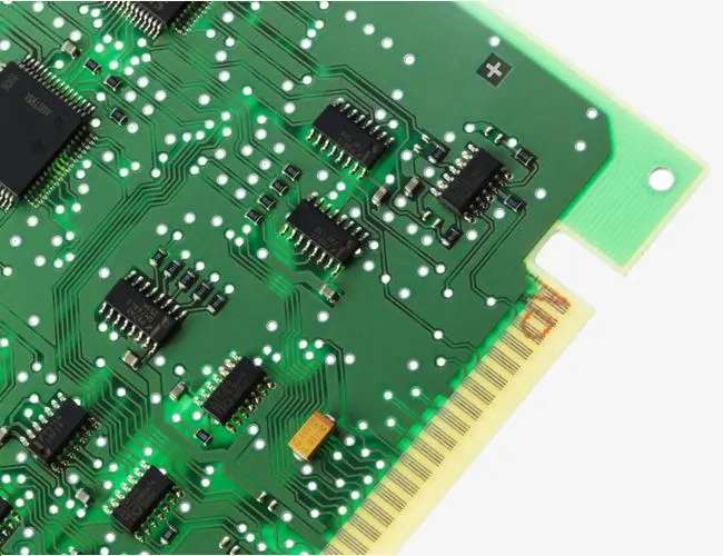
PCB assembly of fast switching switch in electronic industry!
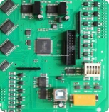
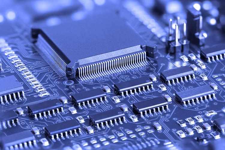
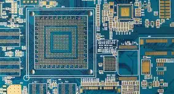
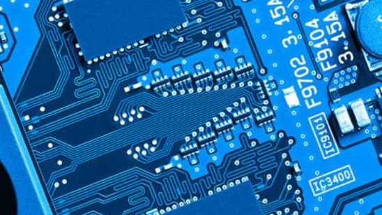
The design of printed circuit board is based on the circuit schematic diagram to realize the functions required by the circuit designer. The design of printed circuit board mainly refers to layout design, which needs to consider the layout of external connections. The optimal layout of internal electronic components, the optimal layout of metal wiring and through-hole, electromagnetic protection, heat dissipation and other factors. Excellent layout design can save production costs and achieve good circuit performance and heat dissipation.
The commonly known printed circuit board or PCB is the most critical component in each electronic device. In fact, they are often called unsung heroes of the modern electronic driven world. After all, this is a component that enables your favorite electronic device to function properly and perform the consumer's favorite actions. For many reasons, the electronics industry benefits from PCB, among which the key is:

Compact design is very effective, especially with the development of miniaturization trend
Easy to test prototypes
Low assembly error
Low noise and interference
Immunization campaign
reliability
Cost effectiveness
Save time
Application of PCB Assembly in Network Switch
One of the areas in which PCB is widely used includes network organization. It is not unreasonable. This is an organization that handles large traffic loads. Network organizations need:
monitor
screen
Summary and
Direct,
A large amount of traffic from multiple links. For such organizations, the data monitoring switch is a valuable device to ensure data access. In turn, these switches require a lot of power to assist them in data aggregation and monitoring processes. This is where PCB components come in handy. The network switch circuit board can benefit from standard and customized printed circuit board components of the network switch, which can meet your customized requirements.
The biggest advantage is that PCB components can support data access switches with multiple ports. It is generally known that multilayer PCBs made of FR4 materials can work well in this case. The biggest advantage it provides is that although the data monitoring process generates a lot of heat, the performance of PCB components will still be affected by the materials used. In addition, if you cooperate with a professional pcb assembly company, you will benefit from its ability to support high-speed switching ports. It turns out that this is an invaluable benefit in itself, as it can help you maintain a competitive advantage.
Capabilities of PCB assemblers
Other functions of professional PCB assemblers include:
RoHS compliant PCB
Lead-free soldering
screen printing
Comprehensive services, including PCB design, PCB prototyping, PCB manufacturing and inspection
IPC Complaint Coating
Online and functional testing
Assemblies compatible with any operating system
Plug and Play Installation
The good news is that the PCB assembly of the network switch can be ready in a short time. This means that you don't have to wait for a long time. As a network organization, you can't afford it. Once the prototype is in place and meets your requirements, you can rest assured that large-scale production operation will not have to face costly errors.
Application of Network Switch PCB Components
Such fast network switch PCB components are widely used in various network systems, including but not limited to:
Network communication system
Large computer network
Network server
Web browser
SNMP Tools
Circuit board processing factory explains the PCB assembly of fast switching switch in electronic industry! With the development of miniaturization trend.


