Rapid construction of new products by PCB assembly prototype
Before starting a complete production run, you need to ensure that the PCB works properly After all, when a PCB fails after full production, it cannot afford costly errors, or worse, it will still detect failures after the product is launched
Prototyping ensures that any problems that may threaten the functionality of the final product are eliminated as soon as possible In fact, multiple PCB prototypes can be run to test individual functions
There are many types of PCB prototypes that can test all aspects. These include:
Visual models: These models are used to illustrate the physical aspects of the design.
Proof of concept prototypes: they are used to test the minimum viability of a product without displaying all its functions
The working prototype has all the functions of the final product and can be used to test its functions.
Functional prototypes: They are very similar to the final product.
According to PCB processing, there are two ways to produce prototypes These include:
Manual through-hole assembly technology
Surface Mount Technology
SMT processing
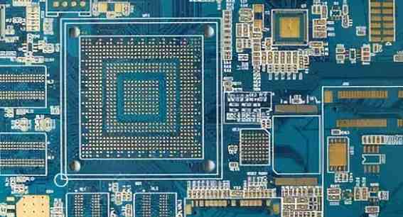
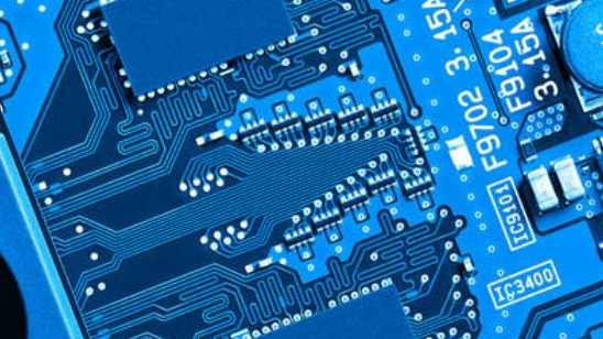
Circuit board

Although SMT processing (surface mount) manufacturing has many advantages, including accommodating smaller components, components placed on both sides of the circuit board, and being less affected by vibration, in the prototype stage, because you are looking for small production runs. This technology is also suitable for situations with limited time and resources. However, it is suitable for less complex designs.
For the following reasons, the overall PCB prototype design helps to quickly build new products:
1. Design changes are allowed. If you think the design seems inappropriate, you can easily change it. Any troubleshooting is easy. This means that you do not have to deal with costly errors in the future. With prototypes, robust testing can be performed to ensure that it works as expected.
2. It ensures quality because it ensures the use of the most effective technology.
3. It allows new products to be tested and revised before production
4. Shorten time. This is possible because it eliminates guesswork and minimizes rework.
5. It provides the ability to test components individually. This is particularly important for complex projects.
Smt processing flow line production process
Surface mounting process
Printing is the first step of the SMT process. Use an automatic mold printer to smear solder paste on the exposed PCB pads. The mechanical fixture inside the printer fixes the PCB and SMT mold together, and the bonding pad on the PCB and the hole on the template are perfectly aligned using the printer's vision system. The thickness of the template, the size of the hole, the pressure and speed of the scraper control the amount of solder paste deposited on the SMT pad on the PCB.
Smt patch
Installation is the second step of SMT. Use the automatic "pick and place" machine to place SMT components on PCB. On this machine, the robot will automatically place the components on the PCB. Before that, the machine needs to be programmed using design files (Gerber files, BOM and CAD files, also known as XY data). The CAD file contains the position and rotation information of all components on the BOM.
Reflow soldering is the third step of surface mount process, and PCB is sent to the reflow furnace Solder paste is used as an adhesive to hold components during heating The oven is programmed using the thermal profile corresponding to the solder paste used Once the solver paste reaches its reflow temperature, it will melt In the case of double panels, each side must be completed separately. Only by strictly following all specified procedures can the quality of PCBA processing be guaranteed


