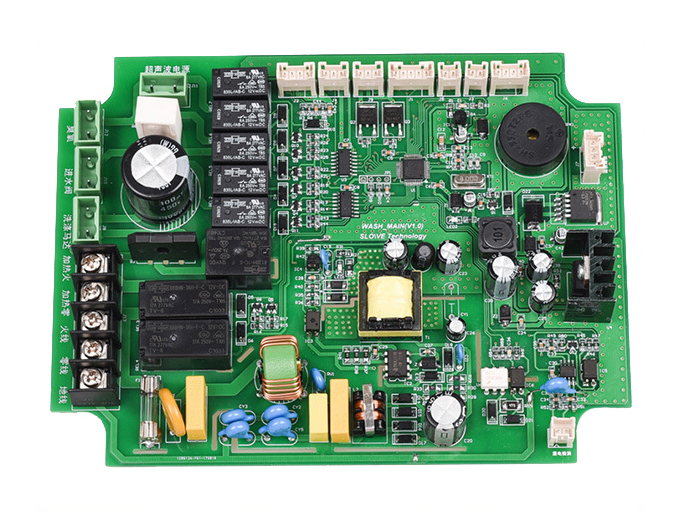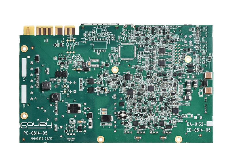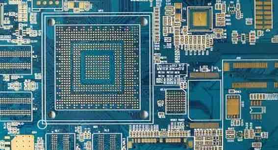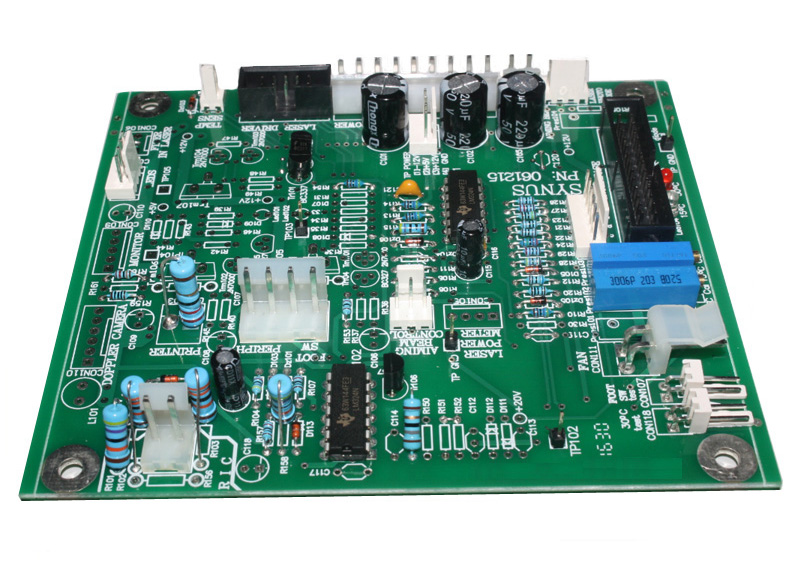
The smart home lighting system is suitable for smart homes and places that require mood lighting and frequent control. The lighting system also includes electronic equipment, such as ballasts, light control or communication units. In order to adapt to the convenience, comfort and other characteristics of smart homes, PCB A small PCB size is required to enhance the usability and adoption of smart home lights in the lifestyle sector.
Component placement, tracking, material selection, and thermal management are combined in the smart home lighting PCB design process to achieve electrical connections on the fabricated circuit board. In order to produce high-quality lighting PCBs with reduced costs, we always adhere to the Design products for manufacturability, thermal performance, and optical performance, because good layout is fundamental to lighting system PCB manufacturing, and the arrangement of parts affects reliability, assembly process, solder joint integrity, and testing. In addition to these considerations, we also consider placement of connectors, active and passive components, thermistors, etc.

on the lighting system PCB, as well as placement of mounting holes, through-holes, and optics. Our team also considers the PCB's material, insulation and contamination that can occur with the PCB in the application, and then they apply the associated creepage and clearance tolerances for long-lasting performance. After designing the lighting system PCB, Kingford will provide free DFM services, analyze the feasibility of manufacturing and provide customers with relevant documents, etc.
Smart home lighting system PCB assembly performance parameters
Certificate: ROHS/ISO9001
Solder mask color: green red blue white black yellow
Copper Thickness: 0.5-3oz
Hole size: 0.2mm
Substrate: FR4
Plate thickness: 1.6mm
Sample: custom pcba prototype
Surface Treatment: HASL\OSP\Immersion Gold
Service: PCB+Assembly+Component


