What is heavy copper PCB? What are its advantages?
High current heavy copper PCB
There are many types of printed circuit boards (PCBs), one of which is a high current PCB in SMT manufacturers, also known as heavy copper PCB. These cells have some useful characteristics for high current and variable temperature applications. Heavy copper PCB can resist higher temperature for a longer time, handle higher current rate and provide stronger connection points.
We provide high current PCBs with heavy copper components ranging from 3 ounces per square foot (oz/ft2) to 10 oz/ft2. If you need higher copper concentration, we can help you use extremely copper PCBs. See what these PCBs can do and why they should be used.
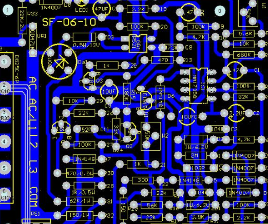
What is a high current PCB?
As the name implies, high current PCB can support higher critical current density than standard circuit board, which may only support double-digit amperage. High current PCB can carry hundreds or thousands of amperes of current, and can withstand higher temperature for a long time. Therefore, they provide a powerful connection point. The unique design of these PCBs has a thicker and heavier copper layer, making PCBs durable.
What is heavy copper PCB?
Heavy copper PCB is a high current PCB, which contains 3 ounces or more of copper in the external and internal layers of the circuit board. Even if the total amount of copper is less than 3 ounces, if the copper thickness of a PCB is greater than 4 ounces/square foot, it is considered as a heavy copper PCB. Copper PCB is typically 10 ounces per square foot or more.
This large amount of copper is used as an alternative method to increase the wire thickness, which is not always feasible. The standard PCB routing for DC motors usually requires a specific width to provide an appropriate power level, taking into account thermal constraints. Thick copper PCB uses thicker wiring to accomplish the same work, but the width will be reduced.
The thickness of plated holes and through hole sidewalls of PCB with thick copper circuit may increase. The manufacturing process is slightly different from that of standard PCB, and special electroplating and etching technologies are used to adapt to the extra thickness of copper. Thick copper PCB can well withstand high temperature (such as welding heat) and corrosive environment. In these cases, the copper PCB can form a non-toxic passivation layer to protect it.
Advantages of High Current Heavy Copper PCB
The main advantage of medium thick copper pcb in smt chip factory is that it can support high current, high temperature and repeated thermal cycle. These factors often cause problems with standard circuit boards. Other advantages of heavy copper PCB include:
Structure: using heavy copper, smt processing chip circuit board can achieve higher density and minimize the number of layers, so as to achieve a simple and durable structure. They can install more conductive materials in less space and achieve stronger mechanical strength for connectors.
Smaller failure rate: High current and increased design complexity will generate more heat. With correct design, the high thermal conductivity of copper enables it to take heat away from the temperature sensitive components of PCB, thus keeping them in a better state.
Production cost efficiency: As a material, copper is a little expensive, but the overall production cost of heavy copper PCB is reduced. Thick copper PCB can be used instead of copper cable to improve cost efficiency. The specific production method also allows heavy copper to be mixed with standard features on the PCB, thereby reducing the number of layers, smaller footprint and saving production costs.


