Matters needing attention in PCBA circuit board assembly and production
1. DFM inspection
DFM check to see all the design specifications of the PCB. Any missing, redundant, or potentially problematic features are looked for.
2. Incoming Quality Control (IQC)
Validate all incoming materials and handle quality issues before SMT assembly begins. Our IQC position will check that incoming materials meet our strict requirements.
Model and quantity according to BOM list
Shape (deformation, broken pins, oxidation, etc.), especially for ICs or other complex components
Use test racks, multimeters and other tools to sample and test incoming materials.
In the event of such defects or discrepancies, we will return all materials received to the supplier or customer.
3. Machine programming - Gerber/CAD to Centroid/Placement/XY file
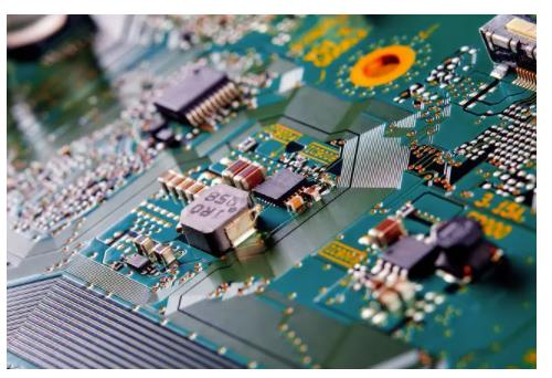
After receiving the PCB panels and components, the next step is to set up the various machines used in the manufacturing process. Machines such as pick and place machines and AOI (Automated Optical Inspection) require the creation of a program, which is preferably generated from CAD data, but is often not available. Gerber data is almost always available, as this is the data needed to make a bare PCB.
4. Solder paste printing
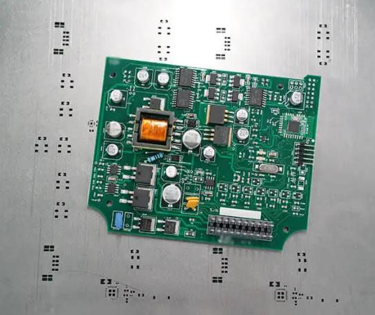
The first machine set up in the SMT production process is a solder paste printer, which is designed to apply solder paste to the appropriate pads on the PCB using a stencil and a squeegee.
5. Component placement
Once the printed PCB is confirmed to have the correct amount of solder paste applied, it moves on to the next part of the manufacturing process, component placement. Each component is removed from the package using a vacuum or gripper nozzle, inspected by a vision system and placed in a programmed position at high speed.
6. Pre-Reflow Automatic Optical Inspection (AOI)
After the component placement process, it is important to verify that no errors have occurred and that all components are properly placed prior to reflow soldering. The best way to do this is to use an AOI machine to check things like component presence, type/value and polarity.
7. Reflow soldering
After the PCB assembly is placed on the board, each piece will be sent through our reflow soldering machine. This means that the solder paste needs to cure, adhering the components to the board. PCB Assembly accomplishes this through a process called "reflow."
8. Automatic Optical Inspection (AOI) after reflow soldering
The final part of the surface mount assembly process is to use the AOI machine again to check the quality of the solder joints for errors.
Checking for these errors and misalignments may involve one of several different checking methods. The most common of these inspection methods include:
Manual check
Automatic Optical Inspection (AOI)
Automated X-ray Inspection (AXI)
AOI inspection
9. Conformal coating
Some finished printed circuit board assemblies have conformal coatings. This usually depends on the customer's product requirements.
10. Final inspection and functional testing
After the soldering and conformal coating steps of the PCB assembly process are complete, a final inspection will be performed by our Quality Assurance team to test the functionality of the PCB. Such checks are called "functional tests". Test software and tools are usually provided by customers, and Kingford can also make fixtures according to customer requirements.
11. Washing and drying
Suffice to say, the manufacturing process can be dirty. Solder paste will leave some flux and need to be cleaned of oil and dirt on the product surface
12. Packaging and Shipping
All PCB assembled boards are packaged (anti-static packaging can be requested) Any unused components are returned according to customer instructions. Additionally, customers receive email notifications when their packages are shipped.


