How to check the quality of PCBA conformal coating
1. Conformal coating
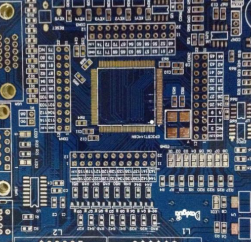
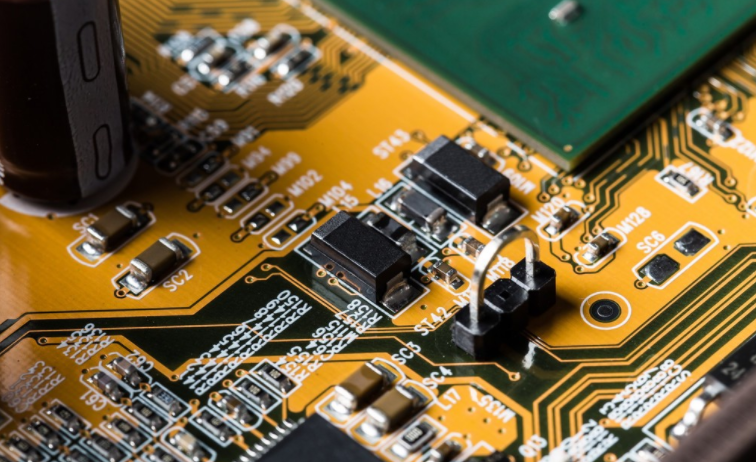
Coated PCBs shall cover printed boards and components transparently and uniformly Whether the coating is uniform depends on the coating method to a certain extent, which will affect the appearance of PCB and the coating condition of corners Dip coated components in SMT wafer processing will have a "deposition line" of paint accumulation, or a small amount of bubbles on the edge of the board, which will not affect the function and reliability of the coating How to check PCB conformal coating
PCB board
2. Coating
The coating on the PCB can be visually inspected. Coatings containing fluorescent materials can be inspected under dark light, and white light can be used as an auxiliary means for coating inspection.
1) Objectives
Polychlorinated biphenyl module has good adhesion; No cavitation or bubbles.
PCBs did not detect sub wetting, dusting, peeling, wrinkles (non adherent areas) cracking, ripples, fish eyes or orange peeling.
No foreign matters; No discoloration or loss of clarity; The coating is completely cured and uniform.
2) Acceptable

The coating is completely cured and uniform; Areas requiring coating shall be covered with coating; Solder mask has no adhesion.
There is no adhesion loss, no gap or bubble, no semi humid, no crack, no wavy line, no fish eye or orange peeling at the bridge of adjacent pads or conductor surfaces on PCB; The foreign matter will not affect the electrical clearance between the components, welding plates or conductor surfaces.
The coating is thin but still covers the edge of the part.
3) Defects
The coating is not cured (showing stickiness)
The area to be coated is not coated.
The area to be coated is lack of coating.
Due to serious loss of adhesion (chalking), voids or bubbles, semi wetting, cracks, ripples, fish eyes or orange peel, the bonding of adjacent conductors or PCB pads results in bridging of pads or adjacent conductor surfaces, exposing circuits or affecting the electric and pneumatic gap between component pads or conductor surfaces. Discoloration or reduced transparency.
3. Thickness of conformal coating
The data of the sample can be compared with PCB or other non porous data, such as metal or glass Wet film thickness measurement is also a method of coating thickness measurement, which is based on the known dry/final coating thickness conversion relationship
The above is the explanation given by the editor of pcb circuit board company. If you want to know more about PCBA, you can go to our company's home page to learn about it. In addition, our company also sells various circuit boards,
High frequency circuit board and SMT chip are waiting for your presence again.


