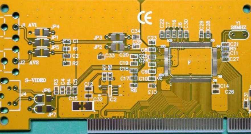
The design of the printed circuit boardis based on the schematic diagram of the circuit to achieve the function required by the circuit designer. The design of printed circuit board mainly refers to the layout design, which needs to consider the layout of external connections. Optimized layout of internal electronic components. Optimized layout of metal wires and through holes. Electromagnetic protection. Heat dissipation and other factors. Good layout design can save production cost and achieve good circuit performance and heat dissipation performance. Simple layout design can be realized by hand, complex layout design needs to rely on computer aided design.
Here to introduce a special for beginners or college students customized a 51 development board PCB design process of actual combat video, from the very familiar 51 microcontroller development board, very intuitive to see a 51 microcontroller development board PCB is how to draw step by step, so that you in the process of learning suddenly awakening, The original PCB design is not a difficult thing!
In order to help you to best learn PCB design, the school of enthusiasts together with Fanyi PCB online training institutions, launched Zheng Zhenyu teach you 1 day play AlTIum 51 development board PCB practical crash series courses, designed for the majority of electronic college students, electronic newcomers or want to * become a high salary electronic R & D engineer, Provide a comprehensive and perfect process of PCB design engineer learning course!
The works produced in the course can be directly taken to production, and then their own debugging, writing programs, and can be taken to participate in the electronic contest, very wide use, is a strong electronic project.
Learning the ability to design PCB circuits independently takes you 3 months to achieve PCB design work experience.
When applying for an electronics position, one of the most common questions interviewers ask is, how many years of experience do you have? Are you familiar with electronic design software? Do you understand the circuit design rules? Will you design the circuit independently? You may not be able to answer, or only answer part of them correctly, but you know little about circuit design, planning and layout rules, or you only know how to do, do not know the implementation principle, rule setting, electrical properties and do not understand.
However, these are all OK, as long as you follow our learning plan, learn step by step, stage training and summary, our course * you can reach the ability of independent circuit design, 3 months to bring you to the level of PCB design engineer!

Course advantage: Rare original course + teacher real-time online tutoring
All courses use online recording and broadcasting teaching, courses set up exclusive VIP QQ group for students, the lecturer team 365 days online to fully answer your learning process of knowledge and difficulties, for you to easily learn PCB design at ease!
In addition, our course also has the following advantages:
1. The quality and quantity of the course content are guaranteed. Compared with offline training, the tuition fee is the lowest;
2. More than 10 years of experience as PCB design engineer, able to solve students' learning difficulties and difficulties;
3. The content is practical, and the teaching content is closely related to the actual work;
4. Package learning package meeting, students can learn repeatedly, support multi-platform viewing;
5. Good after-sale service for the course, and support a variety of ways of "graphic answer + video demonstration" for question answering;
Zheng Zhenyu PCB Design series courses, the content is detailed, easy to understand, through learning this course, you will GET the following skills:
1. Master the basic functions of AlTIum Designer
2. Understand schematic diagram and analysis
3. Understand the basic ideas and process design of 2-layer PCB design
4. Master interactive layout and modular layout
5. Master PCB wiring ideas and skills
6. Understand the output and arrangement of production materials
7. Expansion: I can welding after making physical proofs by myself and further debugging to increase my hands-on ability, which will give me a qualitative improvement and theoretical verification in my university career.
Course features: practical practice, theory as a supplement
1, the whole process - each operation step is recorded and explained, not missing every detail!
2, system integrity - from schematic analysis to PCB import, to how to layout, how to route, to PCB later screen adjustment and PCB production data output.
3. 15% theory +85% actual operation
Course list:
1. Preface
2. Analysis and inspection of schematic diagram
3, PCB import and packaging creation, import solutions to common problems
4. Design and check the specifications of PCB packaging
5. Preliminary preparation of PCB layout
6. Modular layout and layout planning
7. PCB Layout (1)
8. PCB Layout (2)
9. Add and create 3D packaging
10. Class creation and rule setting
11. PCB fan-hole treatment
12. PCB wiring
13. Repair PCB wiring
14. DRC processing and copper repair
15. Adjustment of screen printing
16. Output of the means of production (Gerber)
17. PCB case review;


