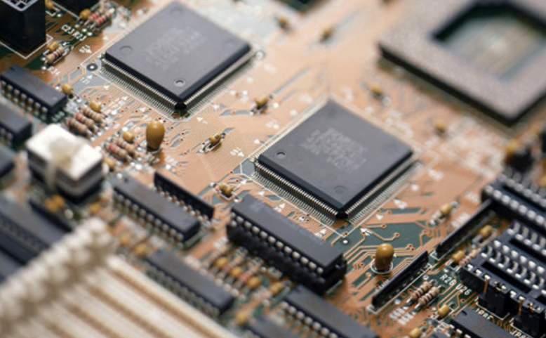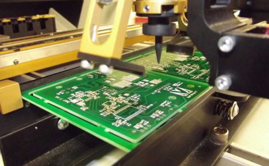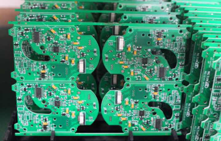
PCB manufacturing process involves a series of processes such as PCB circuit board manufacturing, component procurement and inspection, patch processing, plug-in processing, program firing, testing, aging, etc. The supply and manufacturing chain is relatively long. Defects in any link will cause defects in large quantities of PCBA boards, resulting in serious consequences. Therefore, it is very important to control the whole manufacturing process of PCBA. This paper focuses on the following aspects of analysis.
1. PCB circuit board manufacturing
It is particularly important to hold pre-production meeting after receiving PCBA orders, which mainly involves process analysis based on PCB Gerber files and submission of manufacturability report (DFM) to customers. Many small factories do not pay attention to this, but it is easy to produce quality problems caused by poor PCB design, resulting in a lot of rework and repair work. Production is no exception, need to think twice, do a good job in advance. For example, when analyzing PCB files, for some small and easy to fail materials, be sure to avoid higher materials in terms of structure layout, so that the soldering head is easy to operate when repairing; PCB hole spacing and the bearing capacity of the plate, do not cause bending or fracture; Wiring takes into account key factors such as high frequency signal interference and impedance.
2. Procurement and inspection of components
The procurement of components needs to strictly control the channels, must be picked up from large traders and original factories, and 100% avoid second-hand materials and fake materials. In addition, set up a special incoming material inspection post, strict inspection of the following items, to ensure that components without fault.
PCB: temperature test of reflow welding furnace, no flying line, whether the hole is blocked or leaking ink, whether the board is bent, etc
IC: Check whether the silk screen is consistent with the BOM and store it at constant temperature and humidity
Other common materials: Check the silk screen, appearance, and power-on measurement
The inspection items are carried out in the way of random inspection, and the proportion is generally 1-3%

3. SMT Assembly processing
Solder paste printing and reflow furnace temperature control are the key points. It is very important to use laser steel mesh with good quality and in line with process requirements. According to the requirements of PCB circuit board, part of the need to increase or reduce the steel mesh, or use U-shaped holes, according to the process requirements of the production of steel mesh. The furnace temperature and speed control of reflow welding is very critical for solder paste infiltration and welding reliability, which can be controlled according to normal SOP operating guidelines. In addition, strict implementation of AOI testing is required to minimize adverse human factors.
4, plug-in processing
In the plug-in process, the die design for over wave soldering is the key point. How to use the mold to maximize the probability of good products after furnace is a process that PE engineers must constantly practice and summarize experience.
5. Process firing
In the early DFM report, the customer can be advised to set some Test Points on the PCB board for the purpose of testing the PCB and PCBA circuit connectivity after all components are soldered. If conditions, you can ask the customer to provide the program, through the burner (such as ST-LINK, J-LINK, etc.) will be fired into the main control IC, you can be more intuitive test a variety of touch action brought by the functional changes, in order to test the functional integrity of the whole block of PCBA.
6. PCBA board test
For orders with PCBA Test requirements, the main Test contents include ICT (In Circuit Test), FCT (Function Test), Burn In Test (aging test), temperature and humidity test, drop test, etc., which can be operated according to the customer's test scheme and summarized report data.


