Along with the continuous improvement of the electronic craft level of our country, our country has become a processing plant of the world electronic industry. Surface mounting technology is an important part of electronic advanced manufacturing technology. The rapid development and popularization of SMT processing has played a unique role in promoting the development of modern information industry. At present, SMT has been widely used in the assembly of electronic components and devices in various industries. According to the current situation and trend of the SMT, as well as the technical requirements brought by the rapid development of the information industry and electronic products, the Chinese electronic manufacturing industry is in urgent need of a large number of specialized technical talents with knowledge of SMT.
Technological purpose
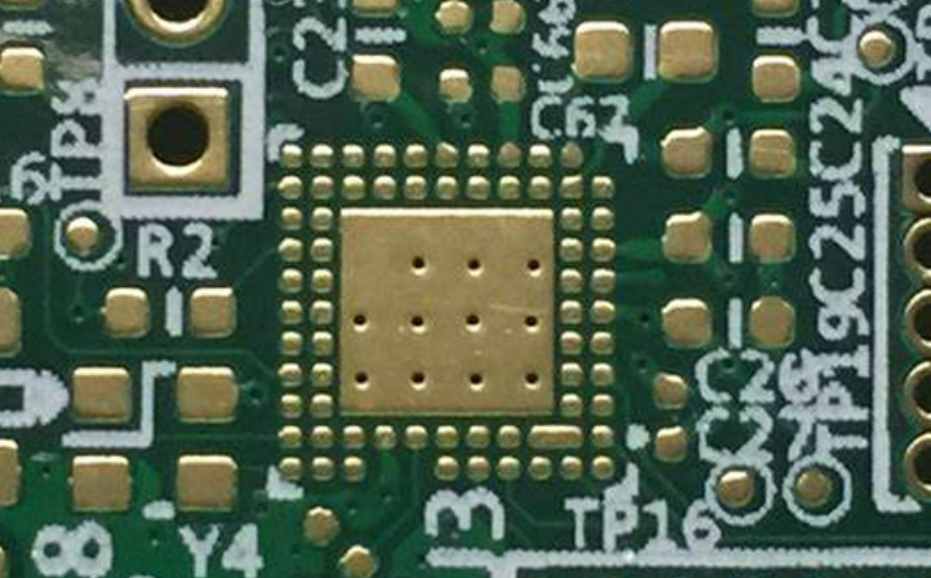
This process is to use a SMT machine to accurately paste the chip components on the PCB board surface of printed solder paste or patch adhesive corresponding position.
SMT process requirements
1. Technical requirements for mounting components
1. The type, model, nominal value, polarity and other characteristic marks of each assembly position number component shall meet the requirements of the assembly drawing and specification of the product.
2. The attached components must be intact.
3. The welding end or pin of the mounted components shall not be less than 1/2 thickness and shall be immersed in the welding paste. The solder paste extrusion amount (length) for general component patches should be less than 0.2mm, and the solder paste extrusion amount (length) for narrow-spaced component patches should be less than 0.1mm.
4. The end or pin of the component is aligned and centered with the welding pad figure. Due to the self-positioning effect in reflow welding, the component mounting position is allowed to have a certain deviation. Allowable deviation range requirements are as follows:
(1) Rectangular components: under the condition of correct PCB design, the width direction of the component welding end width of more than 3/4 on the pad, in the length direction of the component of the welding end and pad overlap, the extension of the pad should be greater than 1/3 of the height of the welding end; In case of rotation deviation, more than 3/4 of the width of the component welding end must be on the pad. Attach to pay special attention to: component welding end must contact solder paste graphics.
(2) Small shape transistor (SOT) : deviation of X, Y and T(rotation Angle) is allowed, but the pins (including toe and heel) must be all on the pad.
(3) Small shape integrated circuit (SOIC) : Allow X, Y, T(rotation Angle) mount deviation, but must ensure that 3/4 of the width of the device pin (including toe and heel) in the pad.
(4) Four-sided flat package devices and ultra-small package devices (QFP): to ensure that the pin width of 3/4 in the pad, allow X, Y, T(rotation Angle) have small mount deviation. Allow the toe of the pin to extend slightly from the pad, but 3/4 of the length of the pin must be on the pad and the heel of the pin must also be on the pad.

Two, ensure the three elements of mounting quality
1. Component correctness requires that the type, model, nominal value, polarity and other characteristic marks of each component with assembly position number should conform to the requirements of the assembly drawing and specification of the product, and should not be pasted in the wrong position.
2. Accurate location
(1) The end or pin of the component should be aligned and centered with the pad figure as far as possible, and ensure that the welding end of the component contacts the paste figure.
(2) The mounting position of components shall meet the technological requirements.
The self-positioning effect of the Chip components of the two ends is relatively large. When mounting, the width direction of the components is more than 1/2 ~ 3/4 lapping on the pad, and the length direction of the two ends as long as they are lapping on the corresponding pad and contact the solder paste graphics. Reflow welding can be self-positioning, but if one of the end is not connected to the pad or no contact paste pattern, reflow welding will produce displacement or suspension bridge.
The self-positioning effect of SOP, SOJ, QFP, PLCC and other devices is relatively small, and the mounting deviation cannot be corrected by reflow welding. If the mounting position exceeds the allowable deviation range, manual correction must be carried out before entering the reflow welding furnace welding. Otherwise, it must be repaired after welding, which will cause man-hours, waste of materials, and even affect product reliability. In the process of production, when the mounting position is found to exceed the allowable deviation range, the mounting coordinates should be corrected in time.
When manual mounting or manual aligning, the mounting position should be accurate. The pin should be aligned with the pad and centered. Do not put wrong. Drag on the solder paste to find the right, so as to avoid the solder paste pattern adhesion, resulting in bridge.
3. Suitable pressure (patch height) suitable patch pressure (Z-axis height) should be appropriate. If the patch pressure is too small, the welding end or pin of the component will float on the surface of the solder paste, and the solder paste will not stick to the component. It is easy to move the position during transfer and reflow welding. In addition, due to the high height of the Z-axis, the component will be dropped from high height during the patch, which will cause the position deviation of the patch. The pressure of the patch is too large, and the extrusion amount of the solder paste is too much, which is easy to cause the adhesion of the solder paste, and the bridge is easy to occur in the flow welding. At the same time, the position of the patch will be offset due to the slide, and the PCB components will be damaged in serious cases.


