Overview of PCB industry
(1)PCB definition
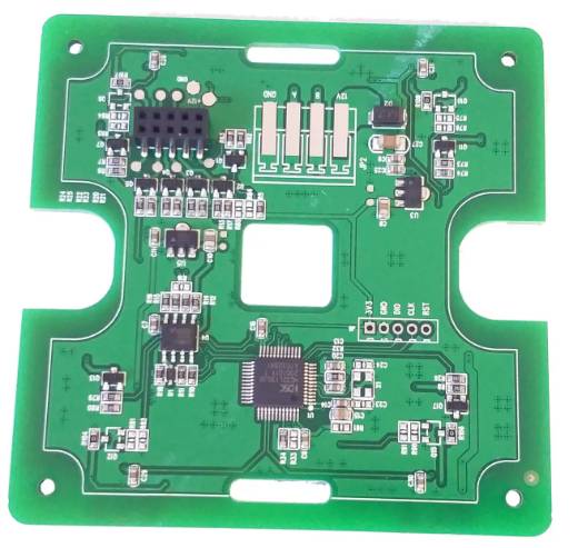
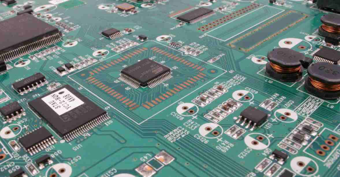
Printed circuit board (PCB) is a finished board made of printed circuit, printed component or a combination of conductive graphics based on the pre-designed circuit schematic. Its main function is to use the board based insulation material to isolate the surface of copper foil conductive layer, realize the connection between electronic components and relay transmission, make the current along the preset line in various electronic components amplification and attenuation, modulation, decoding, encoding and other functions, to achieve the interconnection between electronic components and relay transmission.
PCB is one of the important components of electronic products, small home appliances, mobile phones, to explore the ocean, the universe and other products. Wherever electronic components are available, printed circuit boards are used as supports and interconnects. Therefore, it is known as the "mother of electronic products". If an electronic product is likened to a living organism, then the printed circuit board is the skeleton of the veins connecting the circulation of the circuit.
(2) Development history of PCB
As early as 1903, Mr. Albert Hanson was the first to apply the "line" concept to a telephone switching system. With metal foil cut into wire conductor, glued to the wax paper, but also pasted a layer of wax paper. Prototype of current PCB structure. In 1925, Charles Docas printed circuit patterns on insulated substrates and then successfully constructed conductors for wiring by electroplating. It wasn't until 1936 that Dr. Paul Eisner invented foil film technology. Today's "graphics transfer technology" is followed by his invention, can be said to be the beginning of the real PCB technology. In 1948, the United States officially recognized the invention for commercial use. In the 1950s, copper foil etching became the mainstream of PCB technology and began to be widely used. Perforated metallized double-sided PCBS began mass production in the 1960s. In the 1970s, multilayer panels developed rapidly. In the 1980s, surface-mount printed circuit boards (SMBS) gradually replaced plug-in PCBS. SMB evolved from QFP to BGA in the 1990s. At the same time, multi-chip packaged PCBS based on CSP printed boards and organic laminates are developing rapidly.
Later, PCB board gradually to high density direction development. From the early single-layer, double-layer and multi-layer boards, to HDIMicroviaPCBs, HDIAnyLayerPCBs, and then to the current popular loadlike board, the main feature is the gradual reduction of line width and line distance.
(3) encapsulation level and interconnection density
Semiconductor from wafer to product packaging can be divided into the following levels
• zero-stage packaging (wafer process) circuit design and manufacture on wafer;
• Primary packaging (package process) bonds the chip to the lead frame or package substrate to complete the I/O interconnect and seal protection process, resulting in a packaged device. What we usually call encapsulation is first level encapsulation;
• Secondary packaging (module or SMT process) : a process for assembling components on a circuit board;
• Three-stage packaging (product manufacturing process) : The process of combining multiple circuit boards on a single motherboard or multiple subsystems into a complete electronic product.
Different levels of encapsulation actually represent differences in interconnection density. Wafers usually use lithography. At present, the 7nm process has been mass produced, and the 5nm process has been verified to be ready for mass production next year. The silicon node here represents the gate size of the integrated transistor. The line width and line distance corresponding to the carrier board are usually less than 15μm, and the characteristic size of the chip is amplified to the I/O output corresponding to the characteristic size of the substrate to realize the interconnection between the chip and the substrate. The PCB wire width and spacing corresponding to two-stage packaging are usually greater than 40μm, which is equivalent to enlarging the characteristic size of the substrate to the characteristic size of the PCB to realize signal interconnection.

In fact, there is a middle ground between the PCB and the carrier board. This part is actually the hot carrier board at present. The need for miniaturization of consumer electronics has led to smaller and smaller I/O outputs for the devices used. Take BGA, for example. A few years ago, the dominant spacing for BGA was 0.6mm to 0.8mm. Currently, the device spacing used in smart phones has reached 0.4mm and is moving towards 0.3mm. The 0.3mm pitch design requires 30μm/30μm. At present, HDI is not up to the requirements, and a higher specification type of carrier plate is needed. The class board is the next generation PCB rigid board, using M-SAP process, can shorten the line width/line distance to 30/30μm. Currently, it is widely used in high-end smart phones and some system - level packaging products.
(2) PCB market analysis
(1) Cycle history of PCB industry - four drops
Looking back at history, since the 1980s, various electronic products such as home appliances, computers, mobile phones and communications have emerged one after another, constantly promoting the continuous development of the electronic industry. As an important part of the electronic industry, PCB has experienced four ups and four downs and four industry cycles. In each cycle, the industry was driven by innovation factors to climb, slow growth until recession, and then new factors appeared to push the industry into the next cycle. .
The first stage: 1980-1990 was a fast start period for PCB industry. For the first time, the popularity of home appliances in the world led to the vigorous development of PCB industry. Until 1991-1992, with the peak growth of traditional home appliances and the recession of the Japanese economy, global PCB output declined by about 10%.
The second stage: 1993 to 2000 was a period of continuous growth of PCB industry. Driven mainly by the popularity of desktop computers and the Internet wave, new technologies such as HDI and FPC promoted the continuous growth of the global PCB market scale, and the overall compound growth rate of PCB industry was as high as 10.57%. Demand in the PCB industry was hit by the global economic contraction caused by the bursting of the Internet bubble in 2001-2002, which slowed down demand for downstream electronic terminals. Its production has fallen by about 25% for two years in a row.
The third stage: PCB industry maintained continuous growth from 2003 to 2008 (CAGR=7.73%). This is mainly due to the global economic recovery and the increased demand for downstream emerging electronic products such as mobile phones and laptops, which stimulated the stimulating effect of communications and consumer electronics on the PCB industry. But the outbreak of the financial crisis in the second half of 2008 disrupted the good growth of PCB industry. In 2009, PCB industry experienced a cold winter, the total output value decreased by about 15%.
The fourth stage: from 2010 to 2014, PCB industry showed a slightly fluctuating growth trend (CAGR=2.29%), mainly benefiting from the gradual recovery of global economy and the drive of various downstream intelligent terminal products. With the upgrading of electronic products and slowing demand, the total output value of the industry declined slightly from 2015 to 2016, with a cumulative output value of -5.62%.
At present, PCB industry overall development is slowing down. Starting from 2017, with the emergence of new structural growth hotspots such as 5G, cloud computing and intelligent vehicles, PCB industry is expected to usher in new growth drivers and enter the first industry cycle. Five stages.
(2)PCB product structure analysis
There are many kinds of PCB products, according to the product material, conductive layer number, bending toughness, special performance, process size and other classification, according to the material can be divided into: organic board (phenolic resin, glass fiber/epoxy resin, polyimide, BT, etc.) and inorganic board (aluminum substrate, copper substrate, ceramic substrate mainly rely on heat dissipation); According to the flame retardant performance is divided into: flame resistant type and non-flame retardant type; According to the flexural toughness of the used substrate, Rigid board can be divided into rigid board (RigidPCB), flexible board (FlexPCB) and Rigid-FlexPCB; According to the conductor pattern can be divided into single panel, double panel, multilayer board; According to the process size can be divided into HDI plate and special plate (including carrier plate, packaging substrate, backplane, thick copper plate, high frequency plate, high speed plate, etc.).
Overall, the rigid plate market is the largest, with the multi-layer plate accounting for about 39% of the total output value, and the single/double plate accounting for about 14%. The second is flexible plate, accounting for about 21% of the total output value; HDI boards and packaging substrates account for about 14% and 12%. With the continuous upgrading of global electronic products, technological progress has promoted the continuous development of electronic devices in the direction of lighter, thinner, smaller and mobile. In order to achieve the smaller space, faster speed, higher performance of the goal, the printed circuit board "light, thin, short, small" requirements continue to improve, PCB board structure requirements continue to improve.


