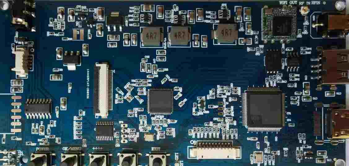
With the rapid development of microelectronics technology, the wide application of large-scale integrated circuit and the progress of micro-assembly technology, the manufacture of printed circuit boards develops towards the direction of layering and multi-function, and the printed circuit graphic wires are fine, microporous and narrow spacing. The mechanical drilling technology used in PCB processing has been unable to meet the requirements, so a new microhole processing mode -- laser drilling has been developed rapidly.
Laser pore-forming principle
Laser is a powerful beam of light excited when rays are stimulated by external stimuli to increase their energy, in which infrared light and visible light have thermal energy, and ultraviolet light has optical energy. Three phenomena occur when this type of light hits the surface of the workpiece, namely reflection, absorption and penetration. The laser spot on the substrate is struck by another optical element, and its composition has a variety of modes, which will produce three reactions with the illuminated point. The main function of laser drilling is to quickly remove the substrate material to be processed by photothermal and photochemical ablation.
Laser drilling process of HDI plate
Photothermal ablation: refers to the processing material absorbs high energy laser, heated in a very short time to melt and evaporate away the principle of pore formation. In this process, under the action of high energy of the substrate material, there is black-burned carbonized residue on the formed pore wall, which must be cleaned before the pore.
Substrate absorbance: Laser success rate and substrate material absorbance has a direct relationship. The printed circuit board is composed of copper foil, glass cloth and resin. The absorbance of these three materials is also different because of the different wavelength. However, the absorption rate of copper foil and glass cloth is higher in the region below 0.3m UV light, but it falls sharply after entering visible light and IR. Organic resin materials can maintain quite high absorptivity in all three segments of the spectrum, which is the property of resin materials.

Photochemical ablation: It refers to the highlighter energy in the ultraviolet region, the result of the action of high energy photons with laser wavelength over 400 nanometers. Such high-energy photons can destroy long molecular chains of organic materials and become smaller particles, whose energy is greater than that of the original molecules, and try to escape from them. Under the condition of external force, the substrate material is quickly removed to form micropores. Because this type of process does not contain hot burning, it will not produce carbonization phenomenon. Therefore, it is very simple to clean up before perforation. At present, there are two most commonly used laser drilling methods: printed circuit board drilling lasers are mainly RF excited CO2 gas laser and UV solid Nd: YAG laser.
CO2 laser pore formation
There are two main drilling methods of CO2 laser hole forming: direct hole forming method and coating mask hole forming method. The so-called direct hole forming process is to modulate the diameter of the laser beam through the main control system of the equipment to be the same as the diameter of the hole on the printed circuit board, and directly process the hole on the surface of the insulating medium without copper foil. The coating mask process method is to coat a special layer of mask on the surface of the printed board, and the coating window is formed by removing the copper foil surface on the surface of the hole through exposure/development/etching process using conventional process methods. The holes are then illuminated with a laser beam larger than the aperture to remove the exposed dielectric layer resin.
Nd: YAG laser drilling process
Nd: YAG is neodymium and yttrium aluminum garnet. UV laser excited by two solid-state crystals. More recently, diode pulsed laser beams have been used to make effective laser sealing systems that do not require water cooling. The laser has a third harmonic wavelength of 355 nanometers (nm) and fourth harmonic wavelength of 266 nanometers (nm), which are modulated by optical crystals. The biggest characteristic of this type of laser drilling is that it belongs to the ultraviolet (UV) spectrum region, and the copper foil and glass fiber composed of copper foil laminate is very strong absorbance in the ultraviolet region, and the light spot of this kind of laser is small and large, so it can strongly penetrate the copper foil and glass cloth and directly into the hole. Because the heat of the above type of laser is smaller, it will not generate carbon slag like CO2 laser drilling, providing a good treatment surface for the subsequent process of the hole wall.
Nd: YAG laser technology is used to process blind and through holes on a variety of materials. A pilot hole is drilled on a polyimide clad copper foil laminate with a minimum diameter of 25 microns. From the production cost analysis, the most economical diameter used is 25125 microns. The drilling rate is 10000 holes/min. Direct laser punching technology can be used, with a maximum aperture of 50 microns. The inner surface of the hole is clean and carbonized, and it is easy to electroplate. It is also possible to drill through holes in teflon copper clad laminates with a minimum diameter of 25 microns, with the most economical diameter being 25125 microns. The drilling rate is 4500 holes/min. No need to pre-etch out the window, the hole is very clean, no additional special processing requirements. There are other materials forming hole processing.
Quality problems in actual production
There is misalignment between the position of CO2 laser drilling and the position of bottom target in the copper window method. In laser drilling, beam positioning system is very important for the accuracy of aperture forming. Although the beam positioning system is used for accurate positioning, the hole deformation flame is often produced due to the influence of other factors. The causes of quality problems in the production process are analyzed as follows:
1. Make the negative of inner core plate welding plate and wire pattern, and the negative of resinous copper foil (RCC) coated with additional layer to open the window, because both will increase and decrease the size due to the influence of humidity and temperature potential factors.
Can be taken to reduce the layout size, most PCB manufacturers make multilayer layout to take 450×600 or 525×600(mm). However, for the processing wire width of 0.10mm and blind hole aperture of 0.15mm mobile phone plate, it is best to use the typesetting size of 350×450(mm) upper limit.
2. The size of the base material itself expands and shrinks when the core plate makes the wire pad pattern, and the size of the inner and outer layer of the base plate material increases after the high temperature pressing paste resin copper foil (RCC).
The laser diameter can be increased: the purpose is to increase the range of copper window covers. The specific method takes "beam diameter = hole diameter +90~100μm. When the energy density is low, it can be solved with one or two more shots.
3. The size and position of the etched copper window will also produce errors.
Adopt the process method of opening large copper window: at this time, the size of the copper window is enlarged while the aperture is unchanged, so the diameter of the laser hole is no longer completely determined by the position of the window, so that the hole position can be directly burned according to the target position of the bottom cushion on the core plate.
4 laser machine itself spot and table displacement caused by the error.
The window opening method is changed from photochemical imaging and etching to YAG laser window opening method: YAG laser spot is used to first open the window according to the benchmark hole of the core plate, and then CO2 laser is used to burn out the hole on the window position to solve the error caused by imaging.
5. Second-order blind hole alignment degree is more difficult, more likely to cause position error.
Second order micro blind hole method: When both sides of the core plate are coated with a layer of resin copper foil (RCC), if it is necessary to layer RCC again and make second order blind holes, the blind hole of "product two" must be aligned according to the target "product one" to form holes. The original target of the core plate cannot be reused. That is, when the "product" into holes and pads, the edge of the plate will also make a target. Therefore, "product two" after the RCC pressed paste, you can through the X-ray machine to "product one" on the target and drill out the "product two" of the four mechanical reference holes, and then into a hole into a line, this method can make "product two" as far as possible to align with "product one".
The pass type is incorrect
According to the accumulation of production experience, mainly because of the quality problems of the substrate forming, the main quality problem is that the thickness of the medium layer is inevitably different after the resin coated copper foil is pressed and pasted. Under the same drilling energy, the bottom pad of the thinner part of the medium layer should not only bear more energy, but also reflect more energy, so the hole wall into the outward expansion of the pot shape. This will bring a series of technical problems to the reliability of high density interconnect structure of layered PCB circuit board. Therefore, must adopt process measures to control and solve. The following processes are mainly used:
1. Strictly control the difference of dielectric layer thickness between 510μm when resin-coated copper foil is pressed.
2. Change the laser energy density and pulse number (gun number), can find out the mass production process conditions through the test method.
3. The removal of rubber slag at the bottom of the hole and broken slag on the hole wall is poor.
This kind of quality problem is most likely to occur, this is due to slightly improper control will produce this type of problem. In particular, it is not possible to guarantee that there are no quality problems when dealing with porous laminated plates on large sheets. This is because the number of micro blind holes on the large row of plates processed is too much (about 60 ~ 90 thousand holes on average), and the thickness of the medium layer is different. When the laser drilling with the same energy is adopted, the thickness of the residual rubber slag on the bottom pad is not the same. Decontamination treatment can not ensure that all residues are thoroughly clean, coupled with poor inspection means, once there are defects, often cause the subsequent copper plating layer and bottom pad and hole wall bonding force.


