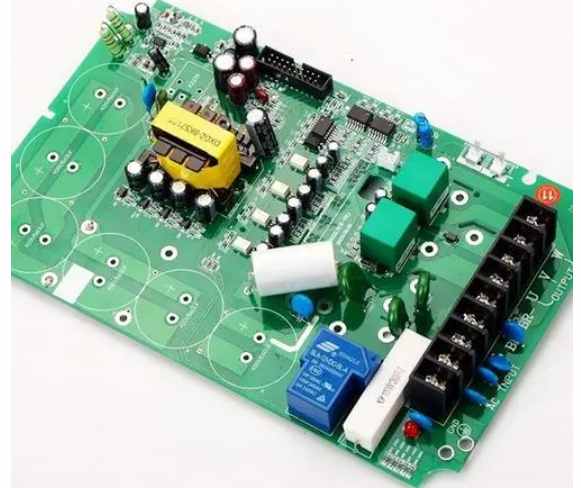
Most of the talk is about wearables, but if the show is about electronics, wearables are there at all. But so far, there hasn't been a product that can fully move consumers to experience. The most worrying thing for consumers is the battery life of wearable devices, which can be used for three or five days if the average performance is a little better and the efficiency is a little more good. Most products need to be charged every day, just like smart phones. The following patch processing manufacturers will explain how to solve the endurance problem of wearable devices and how to reduce the pollution of patch processing.
1. How to reduce the pollution of patch processing
It seems that the processing of electronic products does not produce any harmful substances, but since the country has introduced relevant environmental policies, suddenly development, the whole SMT patch processing unexpectedly has so many pollutants, and the pollution is quite serious pollution, such a situation is terrified many people, as our environment is gradually bad, Environmental protection has become the most popular keyword at this stage. If the environmental pollution has not been reduced in the whole patch processing, it will certainly become the primary target of operation.
In the whole SMT patch, the components and circuit boards are the most harmful, because the welding between the two consumes a lot of power, so it causes great harm to the environment. In order to solve this problem, at present, major enterprises have started to carry out corresponding welding of curing furnace, because the heat insulation of furnace will save energy. But the most important elements are the melting point of the solder, the length of the furnace and the number of hot zones (heating capacity). The heat declared by the device must be removed by the HVAC (heating, ventilation, and air conditioning) equipment, which consumes double the power. At the same time, the welding is directly affixed to the surface of the printed circuit board, and the electrode is welded to the same surface of the components on the pad.
In this way, the through hole on the printed board only plays the role of the circuit connecting wire, the diameter of the hole is only determined by the technological level of the metallized hole when the printed circuit board is made. There is no welding pad around the through hole, so that the wiring density of the printed circuit board is greatly improved. These two methods fundamentally eliminate the harm in the whole patch processing, reduce energy consumption and reduce the harm to the environment

2. How to solve the endurance problem of wearable devices
Since the announcement of Google Glass, wearables have come into the public eye, and have grown remarkably quickly in response to the collection and media fire. By the end of the year, wearables were the most talked about, and only if the show had anything to do with electronics did wearables appear at all. But so far, there hasn't been a product that can fully move consumers to experience. The most worrying thing for consumers is the battery life of wearable devices, which can be used for three or five days if the average performance is a little better and the efficiency is a little more good. Most products need to be charged every day, just like smart phones. In addition, there are other ways to stop optimization. For example, when charging wearable devices, the battery should be filled as much as possible, so as to adequately apply the battery capacity. It has been mentioned that the power design of wearable devices faces challenges.
Because the capacitive capacity of wearable devices is generally relatively small, the battery capacity is widely 40mAh you, have even smaller. In this case, it is not easy to fully charge the battery. As a result, many wearable devices do not use the full capacity of the battery to power the device, so the battery life is greatly affected. Also, the battery leakage current should be small, that is, the standby current of wearable equipment should be small. For example, TI gets Bq25100 and the leakage current is only 75nA. The other is to charge the current and voltage accuracy to be high. As long as the high precision voltage and current can be full of batteries, otherwise the error will be comparable to large. Mentioned Bq25100 can be as low as 10mA or up to 250mA fast charging current stop accurate grasp, while also can complete as low as 1mA charging stop. There are many reasons for the poor battery life of wearable devices. Firstly, the size of wearable devices is relatively small, so they cannot be equipped with large-capacity batteries, which have infinite energy density. Second, wearable devices with Bluetooth, WiFi and other wireless communication modules to facilitate people to connect with other devices, wireless communication is generally more power consumption; Then there are the features that need to be turned on over time.
So is there any way to extend the battery life of a wearable device? In my opinion, it should be possible. In the case that battery data skills have not been significantly improved, we can also extend the battery life through other methods, such as cutting some functions of wearable devices, such as Misfit can be used for six months, Mi Band is also advertised to be used for one month, and their functions are relatively simple. I once heard from a colleague that he bought a wristband that charges and transmits data directly through the audio interface without wireless transmission function, which can also save a lot of power consumption. Making full use of every milliampere hour of the battery is a good way to extend the application time of wearable devices. In addition, the power of the battery can be reasonably utilized through the good power management system. TI latest MicroSiP power module TPS82740. This power module has a feature, it looks like a welding balloon, welded directly to the PCB board. Because it is so small that it must be welded, the board may be integrated with passive components and Buck underneath, and the overall coating is less than 7 mm square. But it supports 200mA input current, has 95% conversion efficiency, the static current is only 360nA, standby current is 70nA. It is exceptionally suitable for wearable applications.


