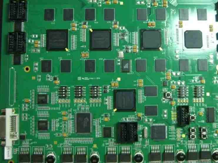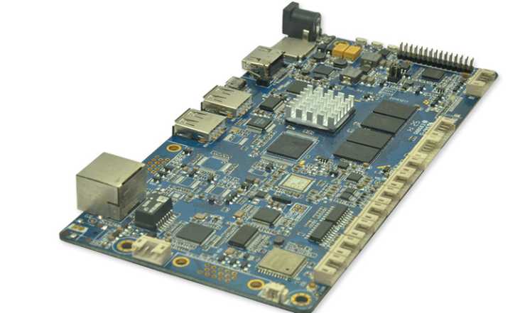
With the increase of IC output switch speed and PCB board density, signal integrity has become one of the important issues in high speed digital PCB design. Components and PCB board parameters, component layout on PCB board, high-speed signal wiring and other factors can cause signal integrity problems, resulting in unstable system work, or even no work at all.
PCB signal integrity problem
Good signal integrity means that the signal can respond with the correct timing and voltage level when needed. Conversely, when the signal does not respond properly, there is a signal integrity problem.
Signal integrity problems can cause or directly cause signal distortion, timing errors, incorrect data, addresses and control lines, system misoperation, and even system crash.
The signal integrity problems of PCB mainly include signal reflection, crosstalk, signal delay and timing error.
1. Reflection
When the signal is transmitted on the transmission line, when the characteristic impedance of the transmission line on the high-speed PCB does not match the impedance of the signal source or the impedance of the load, the signal will be reflected, causing the signal waveform to overflush, underflush and the resulting ringing phenomenon.
Overs hoot is the first peak (or valley) of a signal jump, which is an extra voltage effect over the power level or below the reference ground level;
Unders hoot is the next valley (or peak) at which the signal jumps. Too large overshoot voltage often causes long-term impact of the device damage, downshoot will reduce the noise tolerance, ringing increases the time required for signal stability, thus affecting the system timing.

2. Crosstalk
In PCB, crosstalk refers to the unexpected noise interference caused by electromagnetic energy on adjacent transmission lines through mutual capacitance and mutual inductance coupling when the signal is propagated on the transmission line. It is generated by the interaction of electromagnetic fields caused by different structures in the same area. Mutual capacitance causes coupling current, which is called capacitive crosstalk. The mutual inductance induces coupling voltage, which is called inductive crosstalk. On printed circuit board, crosstalk is related to the length of the wires, the distance between the signal wires, and the condition of the reference ground plane.
3. Signal delay and timing errors
The signal is transmitted at a limited speed on the wire of the PCB circuit board. The signal is sent from the driver end to the receiver end with a transmission delay. Excessive signal delay or signal delay mismatch may result in timing errors and logic device confusion.
PCB design method to ensure signal integrity
In the PCB design process to better ensure the integrity of the signal, can be considered from the following aspects.
(1) Circuit design considerations. Including controlling the output quantity of synchronous switching, controlling the maximum edge rate of each unit (dl/dt and dV/dt), so as to obtain the lowest and acceptable edge rate; Select differential signals for high output functional blocks such as clock drivers; Passive components (such as resistors and capacitors) are connected at the upper end of the transmission line to achieve impedance matching between the transmission line and the load.
(2) Minimize the length of parallel wiring.
(3) Components should be placed away from the 1/O interconnect interface and other areas susceptible to interference and coupling, and minimize the spacing between components.
(4) Shorten the distance between signal routing and reference plane.
(5) Reduce wire impedance and signal driving level.
(6) Terminal matching. A terminal matching circuit or matching element can be added.
(7) Avoid parallel wiring to provide sufficient spacing between wires and reduce inductive coupling.
Signal integrity is an important concept that can not be ignored in PCB design. To ensure that PCB has good signal integrity, engineers need to integrate various influencing factors, reasonable layout and wiring, so as to improve product performance.


