Chip Processing Process
It is easy to understand the point of view of PCBA board manufacturer SMT chip processing: for the capacitance or resistance of electronic products, stick a special machine and weld it to make it more solid and not easy to fall to the ground
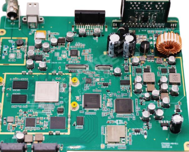
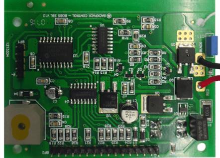
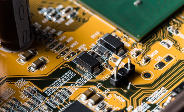
For example, the high-tech products we use now, computers and mobile phones, are closely lined with tiny capacitive resistors on their motherboards. These resistors are pasted through SMT chip processing technology. Capacitor resistors processed by high-tech chips are much faster than manual chips and are not prone to errors.
Surface Mount Technology is the abbreviation of surface mount technology. It is a very popular processing technology in China's electronic industry. Patch processing is a high-tech product processing, so I think it has high requirements for the patch processing workshop.

Polychlorinated biphenyls
SMT processing has certain requirements on environment, humidity and temperature. In order to ensure the quality of the electronic component mounting plant and complete the processing quantity in advance, the following requirements are made for the working environment:
First of all, the temperature requirement is that the annual temperature of SMT plant is 23.+(+) 3 (+), which cannot exceed the limit temperature of 15-35 (+).
Next is the humidity requirement. The humidity in the chip processing workshop has a great impact on the product quality. The higher the ambient humidity is, the more easily the electronic components are affected by moisture, which will affect the conductivity. The welding is not smooth, the humidity is too low, the workshop air is easy to dry, the patch is empty, and it is easy to generate static electricity. In this case, when entering the patch processing workshop, the patch processing personnel also need to wear anti-static clothing, which usually requires the workshop to maintain a constant humidity of about 45% - 70% RH.
SMT technology of PCB manufacturers has two basic processes, one is solder paste reflow process, the other is SMT wave soldering process. In actual production, it shall be separately selected or re mixed according to the type of components and equipment used and the requirements of products to meet the needs of different products.
1. Solder paste reflow soldering process is simple and fast, which is conducive to reducing product volume and shows advantages in lead-free process.
2. The SMT wave soldering process is characterized by the use of double-sided board space, which can further reduce the volume of electronic products. Some of them use through-hole components, which are cheap, but have higher equipment requirements. There are more defects in the wave soldering process, and it is difficult to achieve high-density assembly.
If these two processes are mixed and reused, they can evolve into the assembly process of industrial and electronic products, such as mixed installation.
3. The mixed installation process is shown in Figure 3 The feature of this process is to make full use of PCBA circuit board, which is one of the methods to reduce the installation area, while maintaining the advantage of low cost of through-hole components, which is more common in the assembly of consumer electronic products


