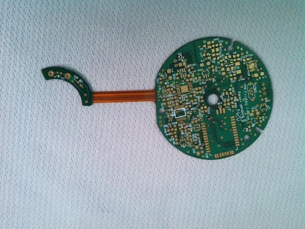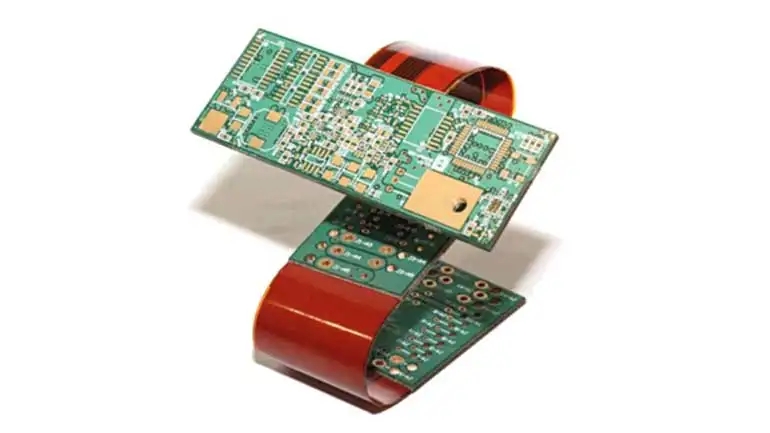
Pcb boards are classified according to the number of layers
PCB manufacturers, PCB designers and PCBA manufacturers will explain the classification of PCB boards according to the number of layers
printed circuit boards, also known as printed circuit boards, are providers of electrical connections for electronic components.
printed circuit board is usually represented by "PCB", not "PCB".
PCB design is mainly layout design; The main advantage of using circuit board is to greatly reduce wiring and assembly errors, and improve the automation level and production labor rate.
Printed circuit board can be divided into single panel, double panel, four layer board, six layer board and other multi-layer circuit boards according to the number of circuit board layers.
Before the appearance of printed circuit board, the interconnection between electronic components depended on the direct connection of wires to form a complete circuit. In the contemporary era, the circuit board only exists as an effective experimental tool, while the printed circuit board has become the absolute dominant position in the electronic industry.
Generally, PCB circuit boards can be divided into single panel, double-sided circuit boards and multi-layer circuit boards according to the number of layers.
1. Single layer PCB board:
On a basic circuit PCB, components gather on one side of the interior, and wires gather on the other side. Since the wires only appear on the inside side, this kind of pcb PCB is called a single-layer pcb PCB (Single sided). Because there are many strict restrictions on the design circuit of single-layer pcb circuit boards (only one side can be used, and the wiring cannot be crossed, so separate paths must be used), such boards can only be used for the initial circuit or the circuit with very simple wiring.

2. Double sided circuit board:
This kind of pcb circuit board has wiring on both sides, but if you want double-sided wires, you must have proper circuit connections between the two sides. Such "bridges" between lines are called pilot holes (via). The pilot hole is a small hole filled with or coated with metal on the PCB of the pcb circuit board, which can be connected with double-sided wires. Because the area of the double-sided PCB is twice as large as that of the single-layer PCB PCB, the double sided PCB buried at the same time solves the difficulty in the single-layer PCB PCB due to the interlaced wiring (it can pass through the guide hole to the other side), and it is more suitable for the more complex circuits than the single-layer PCB PCB.
In order to improve the range of wiring, multi-layer circuit boards use more single or double sided wiring boards. One double-sided PCB is used as the inner layer, two single-layer PCBs are used as the surface layer, or two double-sided PCBs are used as the inner layer, and two single-layer PCBs are used as the surface layer. According to the positioning system and insulating bonding materials, the PCB PCB with alternating conductive patterns interconnected according to the design requirements is called a four layer and six layer PCB PCB, also known as a multilayer PCB. The number of layers of the board does not have multi-layer wiring layers. Under special circumstances, it can enter the empty layer to control the board thickness. Generally, the number of layers is even and includes two layers outside.
The vast majority of motherboards are 4-8 layer structures, but the basic theory of technology can achieve nearly 100 layers of PCB. Most large computers use very multi-layer motherboards. However, since such electronic computers can be replaced by clusters of many ordinary computers, super multilayer circuit boards have been gradually eliminated. Because the layers in PCB are closely combined, it is not easy to see the specific number, but if you carefully observe the motherboard, you can still see that it is a multilayer board.
PCB manufacturers, PCB designers, and PCBA manufacturers will explain the classification of pcb boards according to the number of layers.


